The Gate-All-Around (GAA) Silicon Nanowire Transistors (SNWT) has attracted considerable attention during the last decades as a promising candidate to overcome the scaling issues of MOSFETs at the roadmap of integration circuit process technology. For the purpose of applying the SNWT structures into the fabrication process flow of conventional bulk-silicon (Si) FinFETs for mass production, the fabrication technologies of GAA-SNWTs are necessary to be compatible with current state-of-the-art integration technology. However, the traditional approach to fabricate GAA-SNWTs is to form and release the NW channels in the initial step of the transistor’s fabrication and it causes a series of integration challenges. Recently, scientists from Integrated Circuit Advanced Process Center of the Institute of Microelectronics (IME) of Chinese Academy of Sciences developed a novel technology of NW channel-last (NCL) based on up-to-date high-k/metal-gate (HKMG-last) FinFET process for the first time. The GAA-SNWT with the NCL approach is successfully fabricated with the excellent electrical characteristics in the integration process. 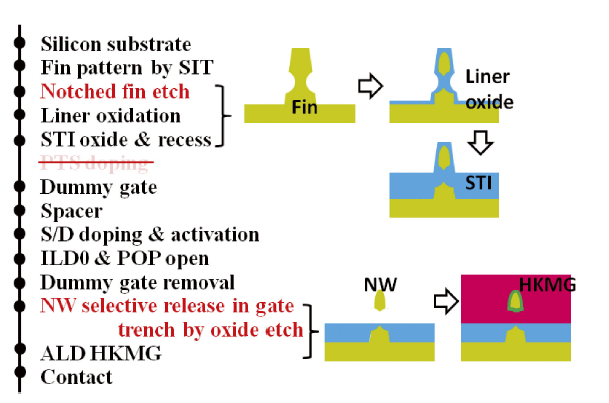
Figure 1. The Fabrication Method of GAA-SNWT with NCL Process Based on the Integration Fow of Conventional Bulk-Si FinFETs. 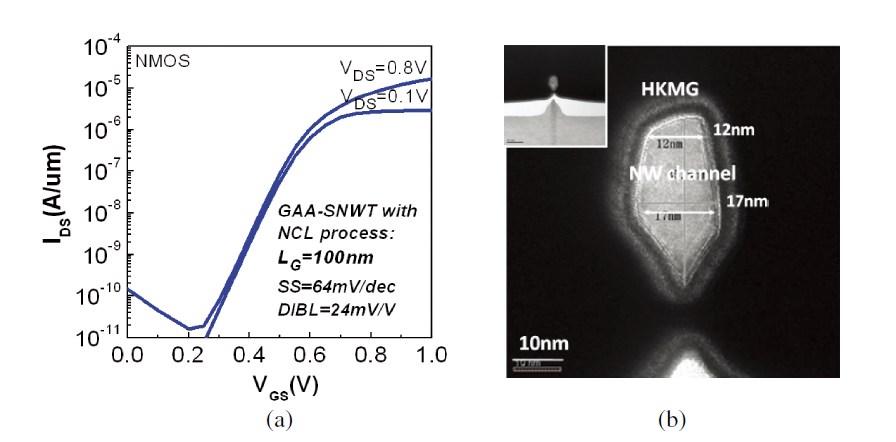
Figure 2. (a) The IDS-VGS Curves of the Fabricated N-type GAA-SNWT by NCL Process with LG ¼ 100 nm; (b) The Cross-Sectional Image of the NW Channel with Multi-Layered HKMG Stacks. Test result showed that the shape of the fabricated NW channel is more like an irregular diamond with the effective nanowire diameter (DNW) of 12 nm∼17 nm. The whole effective channel width (Weff ) is close to 47 nm. The multi-layered HKMG are well surrounding around the irregular channel and demonstrates good film uniformity. It provides a uniform MG effective-work-function (EWF) distribution around whole the channel. The new technology solved long-standing process defects in the large-scale integration process of nanowire devices and provided a promising approach for the integration of nanowire technology into the industrial FinFET flow for mass production in next generations. This work was supported by “16/14nm Basic Technology Research” of national 02 IC projects in China (No. 2013ZX02303). The study has been published in IEICE Electronics Express.(MA X, YIN H, HONG P. Gate-All-Around Silicon Nanowire Transistors with channel-last process on bulk Si substrate [J]. IEICE Electronics Express, 2015, 12(7): 20150094.) CONTACT: Researcher ZHAO Chao E-mail: zhaochao@ime.ac.cn Website of Dept.:http://english.ime.cas.cn/Research/ResearchDivisions/LAB10/ |


