Recently,researchers from Institute of Microelectronics of Chinese Academy of Sciences (IMECAS) carried out new technology on the defect behavior and control method of high-k/III-V and high-k/Ge interfaces.
III-V semiconductor materials, represented by InGaAs, and Ge materials have excellent electron and hole mobility, they are ideal channel materials of high-speed and low-power CMOS devices. The interface is very important to improve the mobility of MOS devices. But the stability of high-k/InGaAs and high-k/Ge interfaces is not good, lots of carrier scattering centers are existed by interface defects, which hamper the achievement of high mobility and affect the final device properties seriously.
Aiming at the core issue, researchers in IMECAS insert an ultra-thin epitaxial InP between the high-k/InGaAs interface, then the interface defects between high-k/InGaAs are transferred to high-k/InP. Combined surface passivation by (NH4)2Sx with high-k Atomic Layer Deposition technology under low temperature, surface oxidation and Phosphorus atom desorption effect during dielectric deposition and annealing after metallization can be suppressed effectively. It does not only decrease the Dit of high-k/InP interface to below 2×1011 cm-2eV-1 (Figure1(a)), but also overcome accumulation capacitance dispersion in high-k/III-V MOS capacitor effectively, the results reach the best level ever reported (Figure1 (b)) .
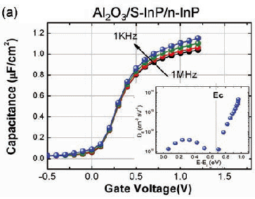
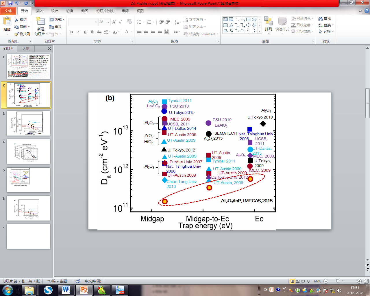
Figure 1 (a) C-V curves and Dit distribution of high-k/InP MOS capacitor made by low temperature ALD technology and surface S-passivation.(b) the Dit of high-k/InP interface is below 2×1011 cm-2eV-1. This result is the best data in high-k/InP MOS interfaces that have ever been reported.(Image by IMECAS)
Different from III-V channel, introducing GeOx layer properly between high-k/Ge interface helps to reduce Dit, however, thermal oxidation with high temperature (400~500oC) and atmospheric pressure is proved not suit to the formation of GeOx interface layer. The main reason is that GeO desorption phenomenon above 420 oC is obvious, which then leads to serious degradation of interface properties. They propose in-situ cycling ozone oxidation under low temperature (300 oC) during high-k atomic layer deposition to solve the high-k/Ge interface problems. It does not only suppress GeO desorption at high temperature, but also get ultra-thin GeOx interface layer with high quality by utilizing blocking effect against ozone during high-k dielectric deposition. Through this method, the lowest Dit of high-k/Ge interface decreases to below 2×1011 cm-2eV-1, reaching the world-class level (Figure 2). Optical and electrical characterization also shows that dielectric leakage and defect density in the dielectric are both decreased. This method provides promising solution for future application of Ge-MOS devices.
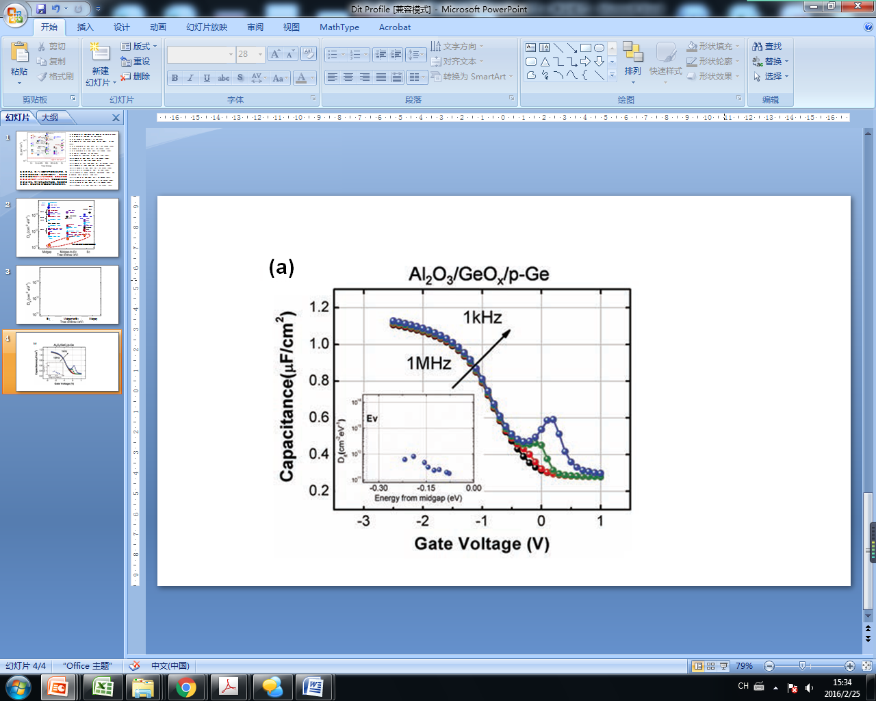
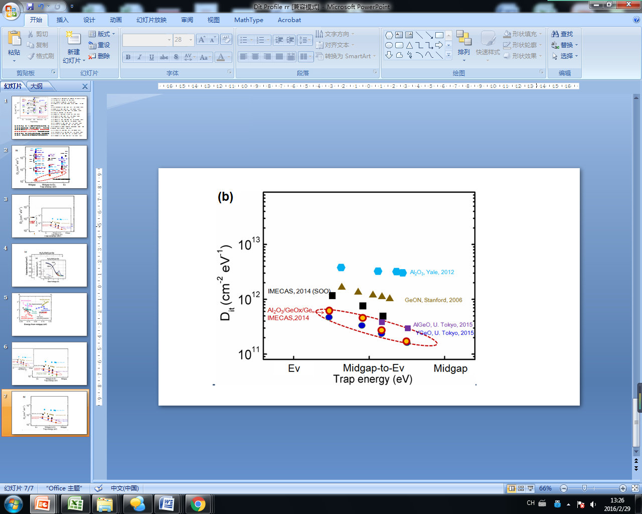
Figure 2 (a) C-V curves and Dit distribution of high-k/Ge MOS capacitor made by in-situ cycling ozone oxidation technology. (b)the lowest Dit of high-k/Ge interface decreases to below 2×1011 cm-2eV-1, reaching the world-class level. (Image by IMECAS)
The above research results receive wide attention from both academia and industry. “Compound Semiconductor”, which is one of the most authoritative magazine in compound semiconductor field, invites Associate Professor Shengkai Wang to write a feature article entitled “Turbo Charging the Channel” for it. The article is published in January / February 2016 (Figure 3).
The research was sponsored by the National Science and Technology 02 Major Project of China, 973 Project and National Natural Science Foundation.

Figure3. Shengkai Wang, Turbo Charging the Channel, Compound Semiconductor, January / February 2016, pp. 36-44. (Image by IMECAS)
Reference:
S. K. Wang et. al. Appl. Phys. Express 8 091201 (2015)
X. Yang et. al. Appl. Phys. Lett. 105 092101 (2014)
X. Kong et. al. IEEE Trans. on Electron Devices Volume:62 Issue: 5 1456 (2015)
S. Li et. al.J. Cryst. Growth 426 147 (2015)
C. Sun et. al. Appl. Phys. Lett. 107 132105 (2015)
C. Sun et. al. ECS Solid State Letters 4 43 (2015)
H. Li et. al. Scientific reports 5 13330 (2015)
B. Gao et. al. ACS Nano 8 6998 (2014)
S. Li et. al. Appl. Phys. Lett. 108 021902 (2016)
CONTACT:
Researcher WANG Shengkai
E-mail:wangshengkai@ime.ac.cn


