Lithography is one of the problems in integrated circuit (IC) technology development because the quality of lithography decides the level of the process and products. The computational lithography group from Institute of Microelectronics of Chinese Academy of Sciences (IMECAS), led by Professor WEI Yayi, carries out a series of researches on the applications of computational lithography used in industrial transfer. The group solves technical problems such as the source mask optimization (SMO), design and technology co-optimization (DTCO), focus monitor mask measuring the focus variation and high reliable alignment.
Source and mask optimization (SMO) is one of the key technologies in resolution enhancement technologies (RET) for advanced technology node. According to the optical imaging model, SMO improves the imaging performance of lithography system by optimizing the source shape, mask patterns and modifying the electromagnetic field distribution of mask. Researchers launched a project called lithography conditions research for key layers in 3D-NAND with Wuhan Xinxin Semiconductor Manufacturing and Cypress Semiconductor Corp. In the project, they proposed a new manufacturing method and did the relevant experiments. The results showed that this new SMO method can not only guarantee the manufacturability, but also make the process window 100nm for single exposure. MEEF is smaller than six and defects are tolerable. The exposure result meets the requirement of industrial production, and solves the problem of lithography process window being too small. This study has been published in J. Micro/Nanolith. MEMS MOEMS.
DTCO is the core technology of lithography technology and chip manufacturing. The standard DTCO workflow is still a blank area in Chinese Foundries. As the IC industry develops to crucial period which is below 20nm technology node, the unidirectional communication from Fab to designer is insufficient to support the development. DTCO is rising in response to the proper times and conditions, which can make a tighter cooperation between fab and fabless. However, this technology is still at the exploratory stage in China.
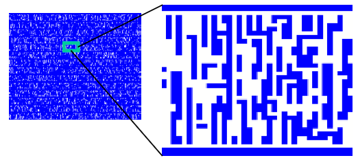
The research group had pioneered research on the applications of DTCO for 10nm and proposed a new DTCO methodology, which contains design rule translation, layout analysis, model validation, hotspots classification and design rule refinement. This technique can be adopted to generate the large scale random layout which guarantees the manufacturability and reflects the new technology node to be developed. This layout can be used in the process exploration and model establishment research before the definition of new technology node is settled. The research results are invited to report in CSTIC 2016. This study has been published in Proc. SPIE 9781, Design-Process-Technology Co-optimization for Manufacturability X.
Control of lithographic process stability is a key problem in 22nm and advanced node. The in-situ monitoring of the focus position change is the significant indicator for achieving the aim of stability control in the microelectronics integration process. As current focus monitoring methods cannot satisfy the requirements of advanced technical node, Prof. WEI’s research group proposes a new focus monitor mask having novel grating structure to measure the focus variation of the scanner. The grating pattern composes of transparent line, opaque line, 180o phase shift groove and 90o phase shift groove with their width ratio equivalent to 1:4:1:2 (Figure 3). By using this structure, one of the first order and one of the second order of the diffraction spectrum are eliminated. Therefore, the lithography image is formed by the interference of the zeroth order and the left positive (or negative) first and second orders, which is more sensitive to the subtle change of focus. Simulations with the lithography simulator PROLITH shows that the sensitivity of the proposed structure is about 0.6026(nm patten shift/nm defocus) ( Figure 2). This means the monitoring accuracy can be improved more than 25%, compared with the conventional phase grating focus monitor (PGFM). This study has been published in Proc. SPIE 9778, Metrology, Inspection, and Process Control for Microlithography XXX.
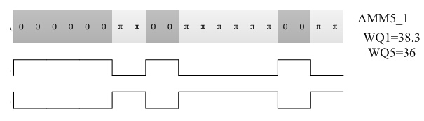
High reliable alignment is one of the key problems in each IC node, and the quality of alignment determines the yield of wafer manufacturing. The group successfully builds a simulation platform to solve the alignment problem. Such simulation platform can also find the relationship between alignment wafer quality (WQ) with some critical parameters, such as determine wavelength, film stack materials and thickness, and alignment mark structures. The simulations are comparable with the real measurement results of ASML (Advanced Semiconductor Material Lithography) TWINSCAN, and they are very similar to the calculations of commercial lithography software. Furthermore, with a simplified algorithm, the group performs some new alignment mark structures in Figure 4 which are better than AH53 and AH74 which used by ASML in diffraction intensity of 1st, 5th, and 7th. In other words, the new design structures have larger WQ in advanced alignment. The designs have been applied for patents, which may show great role in wafer alignment of lithography.