Recently, technological breakthrough is made in collaborative optimization of light source mask in 14 nm CMOS production in the Institute of Microelectronics of Chinese Academy of Sciences (IMECAS). Researchers complete light source optimization in multi-key layers in the back-end process, including Metal 1X、Metal 1.25X、Via 1X and so on. The optimized light source has passed through the wafer data validation. Compared the original light source, key indicators are significantly improved. The stability of the lithography process in advanced node is guaranteed to ensure the progress of the follow-up research and development.
Source-mask optimization (SMO) is an essential resolution enhancement technology in 14 nm and below nodes. Aiming at design rules for a particular layer, mask structure, property and structure of photoresist layer and so on, researcher in IMECAS optimize light source shape, intensity distribution and mask shape simultaneously. Customized light source with Max lithography process window and modified mask shape are obtained by this optimization technique. Figure 1 is a simple example of SMO. The optimized light source can extend the lithography process window significantly; improve the quality of graphic exposure and control deficiency effectively.
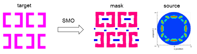
Figure 1: SMO Example
Based on this technology, R & D team led by researcher WEI Yayi in IMECAS cooperated with Semiconductor Manufacturing International Corporation (SMIC), aiming at such difficult structures under the limit size among key layers as end to end line, line end to line, forbidden pitch and so on, successfully solved the lithography problem of corresponding structures, and effectively extended the resolution limit under the current process node. At the same time, researchers used a reduced Gauss model to replace the complex photoresist model, greatly reduced the time period of the first round of SMO work meanwhile the simulating accuracy can be ensured. The simulation results can be well matched with the wafer data. Wafer verification results show that, the optimized light source can significantly improve Depth of Focus (DOF), Mask Error Enhancement Factor (MEEF), Exposure Level (EL), Normalized Image Log Slope (NILS) and other key indicators in the lithography process. Single exposure process window reaches 80 nm. Exposure tolerance reaches more than 10%. Lithography resolution, image quality, and process stability achieved the desired goal, laying a solid foundation for the following research and development work.
CONTACT:
Researcher WEI Yayi
E-mail: weiyayi@ime.ac.cn
Website of Dept.:
http://english.ime.cas.cn/Research/ResearchDivisions/Center1/


