|
|
| A 1053pin FCBGA package has passed test from EDA Center of CAS |
 |
Text Size: A A A |
|
|
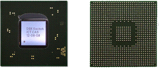
The 1053pin Flipchip-BGA package (shown in Figure 1) developed by EDA Center of CAS has recently passed test, which is designed for the switch chip ‘D5K Switch’ of Institute of Computing Technology of CAS. The chip will be applied in High-performance Computer ‘Dawn 5000A’ supported by 863 Program. On April 16, 2009 the packaged D5K Switch chip has passed DSP test and now is in functional test at Institution of Computing Technology, as has indicated the normal work of the chip.
Currently, in China, the high-end package design and fabrication are completely mastered by several large foreign-invested companies that service only for volume production, while the high-end package service for low volume has always been a bottleneck for the business. Based on BGA package design research and resources in the business, the fast high-end package service system of EDA Center adopts the new procedure to provide the high-end service solutions for small volume. In the project of FCBGA package for D5K Switch, in view of the chip with 32 groups of signals and totally 1053 pins, EDA Center has developed 12-layer HDI BGA substrate. Kyocera has been consigned for substrate fabrication and ASAT for Bumping and Assembly. The package of the chip is the first FCBGA of over 1000pin independently designed in China.
The fast high-end package service system of EDA Center was set up in 2007 to provide perfect package solutions for research institutes and enterprise. In 2007-2008, the system provided the package services for the innovation project of Section I of Institute of Microelectronics, “Optically Readable Non-cooling Infrared Array Sensor” and fabricated the air-tight KOVAR shell with germanium and glass windows.

Figure: D5K Switch Chip in 1053pin FCBGA Package
|
|
|


