At the IEDM conference in Baltimore, IBM researchers indicated that a fully depleted CMOS on extremely thin SOI wafers may be the way to go at the 22 nm node. The approach allows reduced short channel effects, and supports gate length scaling to 25 nm and beyond. The fully depleted technology involves Soitec, which supplies wafers with a thin silicon layer on top of the buried oxide.
David Lammers, News Editor -- Semiconductor International, 12/15/2009
IBM researchers have developed a fully depleted CMOS technology on extremely thin SOI (ETSOI), aimed at the 22 nm technology generation and beyond.
In a presentation at the International Electron Devices Meeting (IEDM) in Baltimore, Kangguo Cheng, lead engineer on the 22 nm device integration team at IBM's Albany R&D center, said the FD-ETSOI process has a 25 nm gate length (Lg) and appears suitable for low-power applications. Besides FETs, IBM engineers created inductors, capacitors, veractors and other supporting devices needed to build system-on-a-chip (SoC) products on the thin SOI substrates.
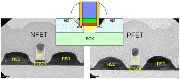
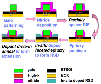
The ETSOI technology incorporates several process innovations, including in situ doped epitaxial (implant-free) deposition of the source/drain and extension regions, and a faceted raised source/drain architecture.
 |
|
The ETSOI technology requires epitaxial deposition of the source/drain and extension regions. |
The approach depends in part on the recent ability of SOI wafer provider Soitec (Bernin, France) to deliver SOI wafers with a silicon thickness in the 6 nm range, said Bruce Doris, manager of advanced device integration at IBM's Albany center. Most of the 300 mm SOI wafers delivered to IBM have an acceptable silicon thickness variation of ±5 Å, although the shipments from Soitec have been in limited quantities thus far.
Technologists face several challenges in scaling planar bulk CMOS to 25 nm gate lengths and beyond. The dopants in the channel are so few that random dopant fluctuations (RDF) cause threshold voltage (Vt) variations. Also, shallower junctions tend to have higher resistance. And voltage scaling has flattened for bulk CMOS, creating power consumption challenges.
"We are reaching the historical ends of those knobs," Doris said at IEDM. The attraction of a fully depleted technology, he said, is that it allows an undoped channel, removing the RDF problem.
For years, technologists have questioned whether FD-ETSOI was practical, largely because of doubts that the critical thickness of the silicon layer above the buried oxide could be kept uniform at <10 nm thicknesses. However, researchers at last year's IEDM from Hitachi Ltd. (Tokyo) and LETI (Grenoble, France) challenged that assumption, showing that Vt variations are not as severe as once feared on ETSOI, Cheng said, arguing that the thickness influence on Vt variation is "overemphasized and exaggerated."
The 25 nm Lg devices on ETSOI technology have record-low Vt variability, Doris said, adding, "We couldn't do this without the SmartCut approach of Soitec."
 |
|
Ghavam Shahidi, IBM |
Cheng discovered that faceted source-drain regions — thought to be a detriment in the past — resulted in reduced capacitance compared with the vertical S-D structures. Doris said Cheng's innovations caught the attention of Ghavam Shahidi, an early advocate of SOI technology at IBM who now is director of silicon technology at IBM's T.J. Watson Research Center (Yorktown Heights, N.Y.). Shahidi added more resources to the ETSOI effort. Ali Khakifirooz, lead device engineer on the ETSOI project, will present further circuit results at the International Solid State Circuits Conference (ISSCC) in San Francisco in February. Doris said further performance advances on the ETSOI nFET are needed, and a progress report may come in a paper at the Symposium on VLSI Technology, scheduled for June in Honolulu.
 |
|
IBM uses faceted S-D structures to reduce parasitic capacitance. |
Cheng and his colleagues worked out a process flow, described in the IEDM paper, that involves further thinning of the already-thinned SOI substrates from Soitec. After shallow trench isolation, a gate-first method is used to form the high-k/metal gate.
After forming the thin spacer regions, in situ boron-doped (ISBD) SiGe is epitaxially grown in both the nFET and pFET regions to form the raised source/drain (RSD). A hardmask is deposited and patterned to expose the SiGe RSD in the nFET regions. The exposed SiGe RSD is removed from the nFET regions by a gas-phase etch process selective to ETSOI silicon. The in situ phosphorus-doped (ISPD) Si:C is epitaxially grown to form the nFET RSD. Annealing drives dopants from the doped RSD toward the ETSOI channel to form the extension junctions. The hardmask is then removed. The final steps involve forming the spacer, silicide, contacts and BEOL interconnects.
At the IEDM conference in Baltimore, IBM researchers indicated that a fully depleted CMOS on extremely thin SOI wafers may be the way to go at the 22 nm node. The approach allows reduced short channel effects, and supports gate length scaling to 25 nm and beyond. The fully depleted technology involves Soitec, which supplies wafers with a thin silicon layer on top of the buried oxide.
David Lammers, News Editor -- Semiconductor International, 12/15/2009


