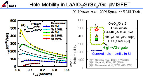
Japan's MIRAI consortium said it has created a germanium p-type transistor prototype with a LaAlO3 high-k dielectric, part of a plan to develop a germanium-based CMOS technology at the 2X technology node and beyond.
Kenji Tsuda, Asia Contributing Editor -- Semiconductor International, 12/29/2009
The Millennium Research for Advanced Information Technology (MIRAI, Tsukuba, Japan) consortium has unveiled a germanium p-type transistor aimed at the 2X generation of process technology and beyond. The Japanese research consortium said the germanium transistor includes a LaAlO3 high-k dielectric, a Schottky barrier source junction, and a shallow junction with a boron stop layer.
The prototype is produced on a bulk germanium material, but later the transistor will be fabricated with a Ge-on-Si substrate. In the early days of the semiconductor industry, germanium was replaced by silicon partly because germanium lacked a stable native oxide, a challenge now being resolved by the introduction of high-k dielectrics. Also, the early germanium transistors could not withstand high-temperature operations because of the lower energy bandgap, which is being resolved in part by the use of strain techniques.
The attraction of germanium is its higher mobility of 4000-5500 cm2/Vsec, depending on the amount of strain, which is almost triple the electron mobility of silicon. According to a calculation by MIRAI engineers, the electron mobility increases as the energy bandgap decreases, which allows strain to impact the germanium bandgap.
The germanium transistor project is being managed by Toshihiko Kanayama of the Advanced Industrial Science and Technology (AIST) agency. In a germanium transistor prototype, the high-k material uses LaAlO3 film with a buffer layer of SrGex. Strontium of up to 10 atomic layers initially is deposited on a germanium surface, and then LaAlO3 is deposited. After a thermal process of 200-800°C, a SrGex barrier layer is created to suppress the migration of oxygen atoms introduced from LaAlO3. When the number of strontium atomic layers increases from zero to 10, the gate leakage current is reduced abruptly while the equivalent oxide thickness (EOT) increases only 0.2 nm due to SrGex formation.
The prototype p-channel MISFET has a peak hole mobility of 481 cm2/Vsec with 7.5 atomic layers, higher than silicon hole mobility. Unfortunately the thicker, 10-atomic-layer film has a surface roughness that leads to mobility reduction.
 |
|
Hole mobility in a germanium MISFET is 4000-5500 cm2/Vsec, depending on the amount of strain.
|
To form shallow junctions at the source and drain, a boron implant is used to suppress the diffusion of phosphorous into the germanium substrate of the n-channel MISFET. A MIRAI engineer said with the formation of the boron stopper layer, no diffusion occurs even with a thermal process of 600°C for 30 minutes in an N2 atmosphere.
Last year, the MIRAI project team reported a Schottly barrier source technology for ballistic transistor operation. The Schottky barrier height is controllable with an arsenic implant using nickel silicide at the source/drain junction. As the arsenic atoms are implanted with 2 × 1014 cm2 to 4 × 1014 cm2, the barrier height increases from 0.1 eV to 0.4 eV.


