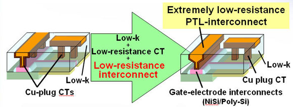
NEC Electronics has developed techniques that create thicker copper contacts for analog and RF transistors implemented on wireless SoCs in a low-power 40 nm technology. The partially thickened local (PTL) contacts cut the resistance and improve the RF Fmax to ~200 GHz for a 40 nm technology. The technique could prove useful for single-chip solutions aimed at next-generation wireless standards.
David Lammers, News Editor -- Semiconductor International, 12/30/2009
NEC Electronics (Tokyo) engineers faced a conundrum in development of the RF circuits created on a 40 nm CMOS technology. The copper contact plugs used in the logic portions of system-on-a-chip (SoCs) wireless products to reduce capacitance were not ideal for the analog and RF portions of long-term evolution (LTE) and WiMax solutions.
Yoshihiro Hayashi, an NEC research fellow, said 4G wireless SoC solutions require high-performance analog and RF transistors, capable of an Fmax of ~200 GHz. Currently, 4G solutions require multichip modules, but efforts are underway to shrink to single-chip solutions.
In 2008, NEC developed a copper double-damascene (Cu-DD) contact structure that reduced the contact resistance, Hayashi said in an interview at the 2009 International Electron Devices Meeting (IEDM) in Baltimore. At that time, NEC expected Fmax performance for the Cu-DD process to improve markedly, but Fmax improved by only ~10%, he said. A conventional CMOS technology with tungsten plugs supported an Fmax of ~155 GHz, while the Cu-DD contacts with a low-k dielectric improved Fmax to ~170 GHz, a less-than-expected boost.
Going back to the drawing board, the team decided to thicken the contacts to the gate electrodes for the RF transistors. The partially thickened local (PTL) interconnect sharply reduced the parasitic resistance to the gates of the analog and RF devices, enabling a higher Fmax.
 |
|
Larger interconnects to the RF transistors reduced parasitic resistance and boosted the frequency. |
By implementing the PTL interconnect on the analog transistors, the input resistance was reduced by 50%, Hayashi said. The result was an Fmax of ~200 GHz for prototypes created in the low-power 40 nm CMOS, while keeping the logic functions in a low-power technology with thinner Cu-DD interconnects.
"It is a very simple idea, but very effective," Hayashi said. "Nobody tried this approach before. Tungsten has much higher resistance. When we switch to copper with a PTL structure we increase the contact area, improve the contact resistance, and boost the Fmax by 30%."
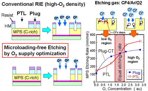
The PTL approach required adjustments to the etching steps. By controlling the oxygen concentration, the thicker contacts were created "at no cost adder," Hayashi said. The reactive ion etching (RIE) steps avoid the microloading effect, and enable both the PTL interconnect and the columnar-shaped copper contacts simultaneously, without additional process steps, he added.
The PTL technology is being considered for either the 28 or 20 nm technology generations, said Hirohito Watanabe, general manager of the NEC Electronics LSI Fundamental Research Laboratory.
 |
|
The RIE steps avoided microloading effects by adjusting the oxygen concentration.
|


