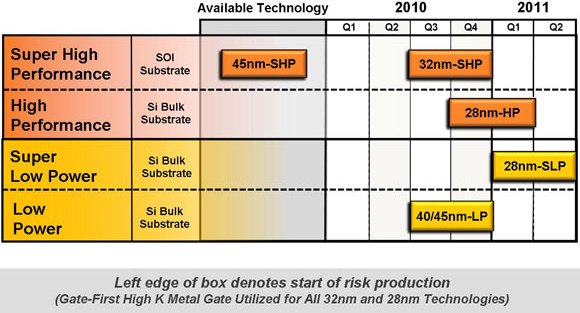
GlobalFoundries is adding Qualcomm to its customer base, starting with 45 nm wafers and moving to a 28 nm LP process that includes high-k/metal gate technology. Prior to the announcement, John Pellerin, director of technology development at GlobalFoundries, said the gate-first approach to high-k deposition has die size advantages over the gate-last approach supported by rival foundry TSMC.
David Lammers, News Editor -- Semiconductor International, 1/7/2010
GlobalFoundries Inc. (Sunnyvale, Calif.) and Qualcomm Inc. (San Diego) announced a foundry and technology-development partnership, including an intention to investigate 3-D packaging technologies.
GlobalFoundries will provide Qualcomm, the largest fabless IC company worldwide, with 45 nm low power (LP) and 28 nm LP wafers, "with an intended collaboration on future advanced process nodes." GlobalFoundries said it plans to begin accepting Qualcomm designs at its Fab 1 in Dresden, Germany in 2010. The foundry's roadmap calls for 45 nm LP shipments to begin in the middle of this year, while the 28 nm LP early "risk" production starts at the beginning of 2011.
The 28 nm LP process includes a gate-first high-k/metal-gate technology, which John Pellerin, director of technology development at GlobalFoundries, said provides a die size advantage over the gate-last deposition process planned by rival foundry Taiwan Semiconductor Manufacturing Co. Ltd. (TSMC, Hsinchu, Taiwan).
 |
|
GlobalFoundries will use high-k/metal gate for all of its 28 nm production. |
At the recent International Electron Devices Meeting IEDM) in Baltimore, sources speculated that GlobalFoundries might switch to a gate-last technology at the 28 nm LP node, partly at the urging of Qualcomm. In a follow-up interview, Pellerin denied that GlobalFoundries was wavering in its commitment to a gate-first approach to high-k/megal gate deposition. Pellerin said the gate-first approach delivers scaling advantages over the gate-last approach, partly due to more restrictive design rules (RDRs) for the gate-last approach.
"We are unequivocally committed to delivering to our customer the best high-k solution, which at 32/28 is a gate-first solution, due to a lot of factors," Pellerin said. The gate-first method offers die size reduction advantages over the gate-last process favored by TSMC, he said. "The scaling potential is a very critical factor. We are getting a lot of feedback from people who are seeking ease of migration to a high-k technology, which delivers a full 50% reduction in die size from 40 to 28."
Pellerin said the gate-last approach is "a metal-fill and polish-intensive process which is very density and pattern sensitive. Customers have to make their designs very regular at the layout level, and have to employ RDRs to get the pattern to look regular. So when they are doing fill and polish to get uniform results, those RDRs impact scaling directly," he said, calling the gate-last approach an "impediment" to the density doubling, which customers expect as they move to a new technology generation.
At the IEDM conference, several technologists said subsequent thermal cycles in the gate-first approach present challenges in terms of Vt stability, impacting performance. Pellerin said while Vt stability was one of the challenges faced in early development of the gate-first approach, there is "nothing intrinsic to our high-k/metal gate approach that carries with it a Vt stability concern. Variation, from a number of sources, is something typically characteristic of early development, and is not representative of the learning and maturity that has transpired from this technology."
GlobalFoundries is shipping MPUs to Advanced Micro Devices Inc. (AMD, Sunnyvale, Calif.), based on its SOI-based 32 nm technology, including the gate-first high-k/metal gate solution. Pellerin said AMD has "very tight variability requirements, and we are able to satisfy their tolerances for Vt variability."
While saying that GlobalFoundries "feels quite confident where we are with this technology," Pellerin said he would not comment on whether GlobalFoundries and other members of the Fishkill Alliance are planning to switch to a gate-last approach at the 22 nm node.
"We are not communicating what our 22/20 architecture is," he said. "The benefit of the alliance is that we can look at what technology options we have that will satisfy the requirements and specifications we are getting from customers. It is not so much whether the solution must be A or B, but how to satisfy the expectations of the customer base. There is not a mandate to switch from our process of record today."
At the 28 nm node, Qualcomm apparently will divide its foundry production among several companies, including GlobalFoundries with the gate-first approach to high-k and TSMC, which in July 2009 said it was supporting a gate-last method. TSMC has been the primary foundry for Qualcomm thus far.
Jim Clifford, senior vice president and general manager of operations at Qualcomm CDMA Technologies, said Qualcomm "needs access to the industry's most advanced technologies." Qualcomm has developed an Integrated Fabless Manufacturing (IFM) model, which builds "tight technical interfaces" among all parties in the IC development cycle, including Qualcomm's multiple foundry partners.
The addition of GlobalFoundries comes at a time when demand for high-end wireless devices is taking off, including mobile systems that operate on the CDMA2000, WCDMA and 4G/LTE cellular standards.
Heterogeneous solution with TSVs
The two companies said they "intend to explore other areas to collaborate on, such as die-package interaction and 3-D packaging technologies." Pellerin said vertical interconnects could serve wireless markets, which seek to marry a logic-process-based IC with complementary die based in non-logic technologies.
Through-silicon vias (TSVs) are not only targeted at mating a logic chip with a memory die, he said. "With TSVs we can really do heterogeneous types of products that can enable high-form-factor, high-function handheld devices. 3-D can gain a lot of leverage in terms of what you can do in a small amount of space," Pellerin said.
ATIC denies UMC interest
GlobalFoundries counts the Abu Dhabi Advanced Technology Investment Corp. (ATIC) as its primary financial backer. This week, the Reuters news agency reported that Chinese-language media in Taiwan were saying that ATIC is interested in taking a stake in United Microelectronics Corp. (UMC, Hsinchu, Taiwan), following the acquisition of Chartered Semiconductor Manufacturing Ltd. (Singapore) late last year.
Asked to comment on any ATIC plans to acquire UMC, Brian Lott, a spokesman for ATIC based in Abu Dhabi, said "those reports are not correct in any way."


