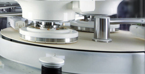
Applied Materials introduced the Reflexion GT system at Semicon Japan. The CMP tool polishes two 300 mm wafers at the same time, using two polishing heads on a pad that is 1.5× larger than today's single-wafer CMP pads. The tool has shipped to several logic and memory vendors. The leading pad vendors are offering 42 in. diameter pads.
David Lammers, News Editor -- Semiconductor International, 11/30/2009
With an eye to reducing the cost of CMP consumables, Applied Materials Inc. (Santa Clara, Calif.) is shipping a tool that polishes two wafers simultaneously on the same platen. The Reflexion GT system, announced on the opening day of Semicon Japan, uses a pad that has 1.5× the area of a conventional CMP pad while polishing twice as many wafers. It also consumes ~30% less slurry per wafer, said Lakshmanan Karuppiah, general manager of Applied's CMP business unit.
CMP consumables are a ~$1.7B annual market, larger than the cost of the equipment itself. As CMP moves beyond logic to memories — polishing several copper interconnect layers on DRAM and flash devices — Applied's customers have been looking for ways to reduce pad and slurry costs. "CMP historically has been one of the costliest steps," explained Sydney Huey, a CMP product manager at Applied. "For a typical logic flow, CMP would account for about $100 per wafer. And that was headed up. Memory is switching from aluminum to copper and, in the logic space, there are more wiring layers."
The Reflexion GT is being tested at several logic and memory customers now; several more systems will ship by the end of this year, said Bill McClintock, general manager of the dielectric systems and CMP group. The tool includes two multi-zone polishing heads, in situ real-time process controls, and two Marangoni vapor drying stations.
 |
|
Applied Materials introduced the dual-wafer Reflexion GT CMP system at Semicon Japan. |
While other CMP vendors have tried to develop dual-wafer CMP tools, and photos of such systems have been passed around, no other vendor has been able to overcome the challenge of duplicating the polishing on two wafers at the same time, according to Applied. Karuppiah said the two Titan Contour polishing heads are controlled independently, and can be configured for a two-step process, or for identical polishing. "It is our real-time control and multi-zone head which enables dual-wafer control," he said.
Applied has worked with the leading pad vendors, several of which are ready to supply pads with a 42 in. surface area, compared with the conventional 30 in. pads used for single-wafer CMP systems.
"We are looking to reduce the cost of consumables," including the cost for pads on a per-wafer basis, Huey said. Based on marathon runs conducted at Applied's technology center, the larger pad will be able to process ~2000 wafers, compared with ~1000 wafers on the single-wafer Reflexion LK system. Those results are independent of the pad set, he added.
"The pad suppliers are on board," McClintock said. "We have worked with all the leaders, and have several options ready for customers. They can use the same slurries they are using today, as well as the same pad conditioning disks, brushing and cleaners. We have worked with the large pad suppliers to ensure that they will not take all the value. Our customers have gotten quotes and have seen the cost savings."
Dean Freeman, equipment analyst at Gartner Inc., said Applied's Reflexion GT sets a new bar for high-throughput CMP systems. Last year, Ebara Corp. (Tokyo) introduced a single-wafer polishing tool with a higher throughput rating than Applied's Reflexion LK system. "Applied went back to work," Freeman said, "aiming at increasing the throughput but also easing the cost of the consumables, which are a big issue with the device makers."
Memory companies will have two to three copper layers on advanced flash and DRAMs. While Intel has nine copper layers, TSMC has up to 12. "This tool is probably going to be a big seller at TSMC," Freeman said. Polishing two wafers on the same pad "is a fairly difficult process to accomplish, which is why we haven't seen it before. We will have to watch the market acceptance, but this could give Applied a huge leg up on the competition."
The CMP equipment market will grow to $984M in 2012, Gartner predicts, up from a depressed level of $459M in 2009. Although Gartner doesn't have precise market numbers for consumables, Freeman said Cabot Microelectronics Corp. (Aurora, Ill.) is the top slurry producer and is ranked second in pads, and Rodel (Phoenix) — part of Rohm and Haas Electronic Materials — is the leading pad vendor and second in slurries.
Although the unit slurry cost does not change, the Reflexion GT will use less slurry on a per-wafer basis because it polishes two wafers at the same time, Karuppiah said. "Customers only have to saturate the pad with slurry once to achieve the required removal rates. That is inherent in the architecture. As they are processing, the slurry byproducts from one head can now go to the next head, which allows the GT to use less slurry to achieve the same removal rate."
In Applied's testing, the GT system used 25% less slurry than the single-wafer LK tool. "Our customers are very good at optimizing consumables, and even a 2% savings is huge to them," Karuppiah said.
Huey said customers will see a 30% fab space savings as well. For a 30,000 wspm fab, assuming 6000 Å of copper incoming and 80 wph of polishing, customers could use seven GT systems compared with 11 single-wafer CMP systems.


