By reversing the electronic assembly process, it's possible to eliminate solder and cut waste. The Occam process is a simplified approach that is reliable and cost-effective.
Joseph Fjelstad, Verdant Electronics, Cupertino, Calif. -- Semiconductor International, 12/1/2009
Occam's Razor is a familiar concept to the scientific community. In short, it teaches that given multiple potential explanations for any observed phenomenon, the simplest explanation is most likely correct. "It is vanity to do with more that which can be done with less," said William of Occam, the 14th century English philosopher and logician whose name is associated with the principle. This inspired a simplified approach to the assembly of electronic products, which will be described in this article.
The new assembly method, known as the Occam process, reverses the traditional approach to manufacturing in that the fully tested and known good packaged IC devices and components are first placed and bound in location by dielectric material or in a dielectric-coated metallic structure. The "dead bug" terminals are exposed and then interconnected using any of several increasingly common build-up circuit technologies used for high-density interconnect (HDI) PCBs. This backward approach to assembly offers an impressive list of prospective benefits including simplified circuit design, reduced layer counts, and improvements in electrical performance, EMI control and shielding, thermal management, energy and material use and costs, design security, resistance to shock and vibration damage, and overall reliability.
For more than 60 years, tin-lead solder was used reliably to interconnect electronic component leads to printed circuits, and made the transition as component technology morphed from through-hole leaded to surface mount. Over time, first pass assembly yields using solder were improved with better processing materials, methods and equipment. Many of those gains, however, were lost during the recent conversion to lead-free solder. As a result, there is growing interest in electronics assembly methods that obviate the need for solder.
Assembly without solder
Those familiar with the current surface-mount assembly process are acutely aware of the difficulties of soldering and that the limitations of the solder process are significant as pitches, which have been steadily shrinking, fall below 0.5 mm. Moreover, the two most attractive component types from a designer's perspective, land grid arrays (LGAs) and quad flat no-lead (QFN) packages, are the most challenging to assembly because of their low stand-off height and the uncertainties of solder joint quality and the efficacy of the cleaning process. There are a whole host of other issues that require attention.
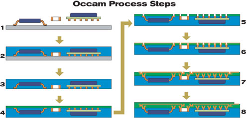
In contrast to traditional surface-mount technology, solderless processing is fundamentally a reversed interconnection process where the traditional PCB is eliminated and subsumed by a post-assembly interconnection process. In the process, standard electronic components (tested and burned-in IC packages, modules and other devices) are first attached to a suitable carrier that can be either permanent or temporary. Then they are encapsulated in place and interconnected using one of several different processes and technologies that are mature, low risk and familiar to the industry. The encapsulated components and other circuit interconnection elements are most desirably interconnected to one another by copper plating circuits to the component lands after they are assembled into their final positions, but the process is not limited, as there are many new developments in conductive inks that could prove suitable. The basic steps of the Occam-type process are shown in Figure 1, which illustrates a reversal of the conventional sequence of creating an electronic assembly, in which components are placed and electroplated with circuits to create electrical interconnections. This has the potential to significantly reduce the time and materials involved in manufacturing.
 |
|
1. The process steps for solderless assembly are relatively few compared to traditional circuit manufacturing and assembly. These include component placement, encapsulation, release (temporary carrier method), first insulation layer, termination access, metallization, circuit patterning and final insulation, leaving access to required interconnection points. Ideal component leads are all copper, which require no special solderable plating. |
During the assembly process, components can first be placed on a temporary carrier such as a removable tacky film or treated surface. Or they can be placed onto a permanent base and components are bonded to it using a permanent adhesive. The film and base temporarily immobilize the components, holding them in place accurately until the structure is encapsulated and the components are permanently locked in place. The result is that an entire array of tested and burned-in components becomes a monolithic assembly. The bottom surfaces of these interconnection terminals can then be exposed by removing the temporary base and film or by making holes in a permanent base by such means as mechanical abrasion or laser ablation.
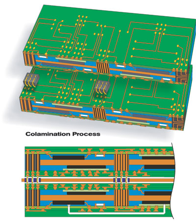
Next, using any suitable metallization technology, such as sputtering or electroless copper plating, the connections to the component terminations are distributed across the encapsulated assembly of electronic components' surface. This can be accomplished using either built-up circuit layers as described, or alternatively by the use of some of the evolving direct-write techniques or by proven direct-wire interconnection techniques. The basic process has other advantages as well. For example, the circuit build-up steps are repeated until all required interconnections are made. In comparison to traditional electronic assembly methods, the Occam-inspired process requires as few as one-third the total number of major and minor process steps for the simplest form assembly. Moreover, the assemblies may be processed back-to-back for greater component density and can be joined together to create more complex electronic structures as illustrated in Figure 2.
 |
|
2. When plating of connections is deemed most appealing, other solderless assembly methods remain possible and of potential interest. One technique involves the use of a pattern of conductive and nonconductive adhesives that correspond to the terminations and insulating areas of the assembled component carrier. |
Efforts to embed discrete device components such as resistors and capacitors into printed circuits have been ongoing for years, but the basic idea of embedded passive function goes back to the 1970s. Efforts to embed bare chips into substrates extend back to the 1980s, with work done at Unistructure and AT&T, later at General Electric, and now at many companies around the globe. Recent efforts to embed passives have largely been undertaken to increase surface area for better and easier soldering and cleaning. Experience with the embedment of bare (unpackaged) IC chips in the past has spotlighted the important issue of known good die (KGD) and yield loss. To overcome these limitations, it is deemed necessary to use packaged and burned-in ICs, preferably having a common base grid pitch, which will greatly facilitate circuit design and layout.
The general objectives of solderless assembly can also be achieved by means of colamination processes that were developed in the 1990s for multilayer PCB manufacture (Fig. 3).1 In such processes, a "programmed" bonding layer comprised of an insulating adhesive layer with openings filled with a conductive adhesive or sinterable alloy paste is used to join a "component layer" to a PCB in a lamination step. One advantage of this is that components can potentially be functionally tested as a system in situ with a suitably designed testing system, especially one having a standard grid that would allow for a universal test.
 |
|
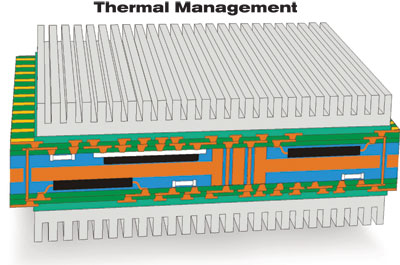
3. Components can be assembled back-to-back or even placed on a heat pipe or spreader, as shown here, for greater component density. The assemblies can be subsequently joined together with mezzanine connectors on or in a metal carrier to create more complex electronic structures and systems. |
Benefits of solder-free assembly
There are numerous advantages to solderless assemby. The most fundamental advantage is avoiding the high-temperature lead-free solder process and its potentially damaging effects. Eliminating solder resolves concerns of component moisture sensitivity level (MSL) and the potential for "popcorning," which is the explosive outgassing of entrapped moisture in packages during reflow. It also eliminates the need for proper dry storage, special handling, prebaking and accurate hold-time recordkeeping. The process also allows the use of components that would be easily damaged at lead-free soldering temperatures (such as aluminum electrolytic capacitors, certain optoelectronic devices, etc.). Another important prospective advantage of solderless assembly is that heat spreaders, heat sinks or even heat pipes can be embedded directly into or made an integral part of the assembly. All are possible because no high-temperature soldering process is required (Fig. 4).
 |
|
4. Thermal management is becoming increasingly important, and yet is often neglected until after circuit fabrication and assembly is complete, resulting in a magnified challenge. In contrast, solderless assembly processing offers the opportunity to address thermal issues at the front of the process rather than as an afterthought. |
Circuit patterns must still be generated for Occam-type assemblies just as they are with standard soldered assemblies, although a number of design constraints can be relaxed. For example, the need for large component pads or lands that are required for soldering the components to the PCB is eliminated, so space-wasting and performance-sapping terminations can be minimized. These assemblies are highly amenable to implementation using the interconnected mesh power system (IMPS) design approach developed by researchers at the University of Arkansas or a similar power mesh concept developed at HP.2,3 These innovative wiring architectures could significantly reduce layer count requirements. These technologies were developed with multichip modules in mind, and largely depend on chips having relatively standard pin outs using a standard grid. This can be accomplished with redistribution, however. Unfortunately, IC design is anything but standard and die shrink is the rule, which makes standardization nearly impossible. In contrast, IC packages are ruled by standards, and if the designer consciously locks into a standard base grid, substantial benefits can be derived.
For example, combining the IMPS design concept with components having leads of the same I/O pitch, coupled with Occam-type processing, creates a direct HDI interconnection to device terminations — a combination that can support requirements for I/O connections up to 400 I/O cm2.4 Beyond increased density and layer reduction, the method offers lower noise and crosstalk, based on reported measurements.5 Moreover, because the packages are embedded, the components are virtually immune to shock and vibration. A recent report by David de Maio at the National Physical Laboratory in England indicates that 80% of the failures in lead-free soldering are related to shock and vibration.6 Finally, the completed assembly can be jacketed with metal to create a near-hermetic assembly. The same jacket can also provide complete electromagnetic interference (EMI) immunity for assembly.
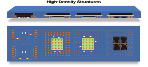
Higher-density structures are possible with the Occam process, because components can be more densely tiled with even component edges potentially abutted since cleaning flux from under the components after assembly is not a requirement. And since the solderball typically represents half of the seated height of a mounted component, removal of solder serves the object of making electronic assemblies thinner. Even so, the process allows for larger components to overlap smaller components that can be placed under them and still directly interconnect to the circuits (Fig. 5).
 |
|
5. Solderless assembly opens the door to new component layout configurations that aren't possible using traditional solder-based methods — especially with higher-temperature lead-free solders. This image shows several potential package-under-package (PuP) variations of components that are overlapped, with some components residing completely in the shadow of others. |
While there are many compelling benefits of solderless assembly, the question of rework and repair is inevitably raised relative to a process where components are embedded and interconnections are plated rather than soldered. However, that question is perhaps best addressed by first asking why rework and repair is necessary. The answer is clearly that the soldering process is imperfect and causes many of the problems and failures in electronics. Shorts and opens are accepted as inevitable outcomes of the soldering process, so rework is expected. In a study by Agilent of 1 billion solder joints, depending on how the data is interpreted, up to 97% of defects are related to the soldering process — with shorts and opens accounting for a full two-thirds of all defects.7 Faulty solder joints are a leading cause of field failures. Plating technology is far more robust and interconnections can be made at very small feature sizes. Via failures are rare, especially if not exposed to lead-free solder temperatures. A good question to ask on this topic: Can the money that is being spent to find and repair defects related to soldering be better spent deploying alternative processes that are less horizon-limited than solder?
Rapid prototyping without solder
Although the focus of this article has been on the potential for volume production, the potential of the technology for rapid prototyping should be of high interest to those seeking to move products rapidly to market. There is presently interest and activity to build a machine that will take care of all aspects of an Occam assembly in a relatively small area by adapting various technologies, both current and evolving, which can be brought together to create better assemblies in a matter of hours rather than the typical cycle of weeks or months. There are, for example, numerous types of machines that can create 3-D structures by layering polymers and/or metals.
 |
|
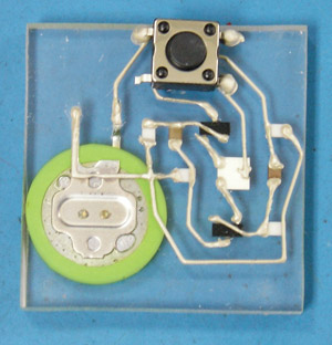
6. This is an example of a simple rapid prototype Occam assembly. Its components were encapsulated and silver ink circuits were drawn using a programmable dispensing tool in place of an inkjet printer. Note that the battery is also embedded and easily survived the curing process. The switch was attached for this demonstration using a conductive adhesive by a dome switch that would normally be used to reduce assembly height. (Source: Promex Industries) |
These same concepts can be used for Occam-type structures. In such cases, a component set could be placed on the surface and scanned with a laser to create a database for the 3-D carrier constructed using a rapid-prototyping tool into which the devices are later placed. The components are bonded in place in the carrier, depending on the process, and the circuits can then be formed and/or written directly onto the component terminations using many different prospective methods such as a programmable dispenser or inkjet printer loaded with conductive ink. The assembly can be coated with an insulating material for protection. Multiple layers can be "written" in this fashion by providing openings for contacts, which is currently being done in the form of a solder mask. An example of a simple single circuit layer produced on the floor of a contract assembler using existing equipment is shown in Figure 6.
Conclusion
The improved approach to assembly offered by the Occam-type process gives OEMs a new choice for producing products in the face of growing concerns about the efficacy and reliability of high-temperature lead-free soldering and its resulting products. This new approach should prove a highly reliable and cost-effective approach to electronic assembly and redefine the circuit manufacturing processes in a way that adds significant value while reducing overall costs and increasing reliability — and also easily clear hurdles put in place by the EU's RoHS legislation.
Test vehicles of different types are being defined, refined and designed at this time and the full qualification process will soon be underway, thanks to the efforts of progressive companies in the electronics interconnection community around the globe.
Given the promise of lower cost, better reliability, reduced supply chain, faster time to market, less waste, virtually automatic RoHS compliance with even greater environmental friendliness, this process is being given serious consideration by major OEMs. What remains to be seen is how quickly it can deliver its lofty promises to users in need of a viable alternative to lead-free solder.
| References: |
-
J. Fjelstad et al., "Manufacture of High-Density Interconnection Substrates by Colamination of Inner Layers and Programmed Interconnection Joining Layers," Circuit World, 1999, Vol. 25, No. 3, p. 9.
-
L. Schaper et al., "Comparison of the Interconnected Mesh Power System and Buried Stripline Interconnect Topologies," Proc. 2001 Int. Conf. High-Density Interconnect and System Packaging.
-
H. Holden, "A Design Technology Innovation — the Power Mesh Architecture for PCBs," The Board Authority, Circuitree, December 2000, Vol. 2, No. 4, p. 42.
-
Personal communication with Happy Holden.
-
L. Schaper et al., "Comparison of the Interconnected Mesh Power System and Buried Stripline Interconnect Topologies," Proc. 2001 Int. Conf. High-Density Interconnect and System Packaging.
-
D. de Maio, "High-Frequency Vibration Tests of Sn-Pb and Lead-Free Solder Joints," Proc. IEMRC/TWI Technical Seminar, "Developments in Interconnection, Assembly and Packaging," December 2008.
-
S. Oresjo, "One Billion Solder Joints and Counting," Circuits Assembly, February 2001, p. 26. |


