|
Diffractive optical elements are becoming increasingly important for use in lithography and inspection equipment, especially as illumination demands call for more complex DOE designs.
James Carriere and Todd Hudson, Tessera Inc., Charlotte, N.C. -- Semiconductor International, 12/1/2009
Diffractive optical elements (DOEs) are commonly coupled with today's state-of-the-art semiconductor equipment to provide off-axis illumination, speckle management or beam-splitting solutions. Their role in providing resolution enhancement is becoming increasingly important as extreme ultraviolet (EUV) lithography continues to be delayed. However, the required illumination for the source mask optimization (SMO) routines being used to extend optical lithography increases the complexity and performance demands on DOEs.
Fortunately, projected requirements for DOEs still do not approach the full number of degrees of freedom (>107) intrinsic in semiconductor equipment devices. This article discusses how DOEs work, how they are designed and produced, and what they can achieve in semiconductor applications.
Initial specification and design process
Light can be manipulated in three distinct ways: reflection (mirrors), refraction (lenses) or diffraction (holograms). DOEs are a specialized form of computer-generated hologram (CGH). Analytically determined surface structure is used to redirect incident light into desired diffraction orders, which are defined by gray-tone target images made up of a grid of pixels. Standard grid resolutions in the deep UV region are on the order of 200×200 pixels, but depend on various parameters of the excimer laser source selected for the application.
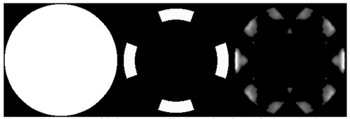
In terms of achievable gray levels in the target image, Tessera's standard process uses 255 discrete gray levels to maximize both functionality and manufacturability. Examples and results of this full gray-tone manufacturing capability have been demonstrated.1–4 By combining the pixel resolution with the discrete gray levels that are available, >107 degrees of freedom are available for optimizing the source illumination. These are only beginning to be fully employed for high-resolution, pixilated designs by recent SMO routines. Some examples of both standard and freeform design targets are shown in Figure 1.
 |
|
1. Examples of design targets used in the creation of DOEs for the semiconductor industry include (left to right) conventional illumination, quadrupole illumination and a complex freeform illumination. (Source: Mentor Graphics) |
The specified target image is used as an input to an iterative design algorithm to calculate the optimal phase profile for the corresponding CGH. When a Fourier transform is applied to the CGH, the result is a simplified representation of the specified target that will be produced by the manufactured DOE. The CGH phase function needs to be further modified for successful operation in a lithography system, with the final result being a DOE that creates the off-axis illumination (OAI).
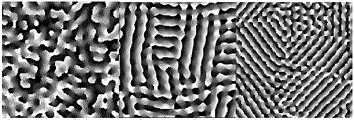
The DOE is created by transferring the modified CGH phase profile into a glass wafer substrate using customized photolithography and etch procedures. Close examination of the DOE reveals freeform fringes that typically bear no resemblance to the output pattern they are designed to create, due to the Fourier transform relationship between the pattern and the DOE (Fig. 2).
 |
|
2. Phase profile images output from Tessera's iterative design algorithm, which corresponds to the design targets ofFigure 1. |
Fabrication procedure
The exact method of fabrication depends on the type of application. Initial prototypes can use direct-write approaches, but to achieve the best part-to-part repeatability required by the standards set by the semiconductor industry, Tessera frequently employs a 2N process. The ideal continuous phase profile is quantized into 2N phase steps, varying from 0 to 2π, and patterned with optical lithography steppers and scanners.
The required tool set may vary, depending on the complexity of the design. Exacting levels of manufacture can be achieved through the use of scanners, thanks to the imaging and overlay capabilities they provide. Also, because the pattern is transferred to a reticle, the initial DOE can be exactly copied and used on multiple lithography lines when qualified for production. This level of DOE repeatability is essential for process portability, without additional process development or customization. Each pixel in the pattern is defined for intensities varying from full power to off, and is programmed to be consistent, regardless of the number of DOEs of a particular design or the amount of time that has lapsed between manufacturing runs.
The number of phase steps for the DOE is determined by the required feature sizes needed to produce the pattern and the desired transmission efficiency. The larger the diffracted angle that is needed from the DOE and the more phase levels that are used, the smaller the minimum feature size that must be produced. Tessera routinely fabricates DOEs with a minimum feature size that is a fraction of a micron, with multiple choices of tool sets available to best match the requirements of each individual application.
Two-phase or eight-phase levels are chosen for most applications. A binary or two-phase level design is generally chosen when the required diffraction angle is large, requiring a very small minimum feature size (<1 μm). Binary designs have a typical maximum efficiency of ~81% (not including reflection losses) and must have mirror symmetry. Eight-phase level designs are most common because they provide the best balance between efficiency and functionality. Eight-level designs can achieve up to ~94% efficiency and do not require the design to be symmetric.
On rare occasions, four-phase levels are the best choice when the required feature size for an eight-level design is too small. The maximum efficiency in this case is still only ~81%, but the design no longer needs to be symmetric. Sixteen or more phase levels can be encoded, but have diminishing returns on efficiency with only a 1–2% increase over the equivalent eight-level design.
Some designs benefit from non-binary encoding, using three- or six-phase levels. The exact efficiency will be dependent on the design — more complex target patterns frequently have lower efficiencies. Fortunately, a more accurate efficiency estimate can be predetermined during the design simulation stage.
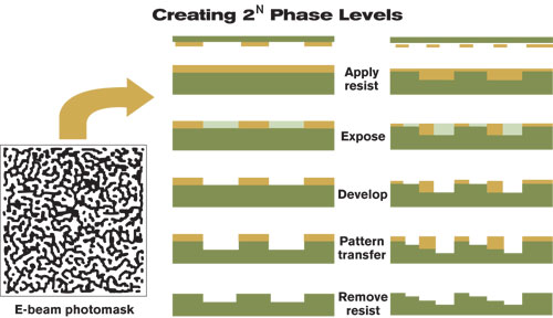
For a nominal fabrication process, the design is first established and quantized into 2N phase steps. The corresponding patterns can then be separated into N layers that are encoded on reticles. The shallowest layer, typically corresponding to the finest features, is patterned first to minimize structural effects on the fidelity of the patterned features. Once the first etch is completed, the remaining photoresist is removed and a new layer is spun over the etched surface before patterning and etching the second layer. This process is repeated N times across the entire substrate to approximate the continuous phase profile as closely as needed (Fig. 3).
|

|
|
3. The photolithographic process used to create the 2N phase levels of the DOE.
Once all layers have been patterned and etched into the substrate, the wafer is diced to the appropriate form factor for each part. The advantages and disadvantages of manufacture at the wafer level for DOEs are the same as in the rest of the semiconductor industry. Economies of scale can be realized for multiple elements to reduce overall production costs, while maintaining excellent part-to-part repeatability through the copy exact nature of the manufacturing procedures. Each part is rigorously tested on customized in-house testing equipment to qualify its functionality in the final system.
Often, the final step in the manufacturing process is the application of an antireflective coating to both surfaces of the DOE. This coating step is required to maximize transmission efficiency, and requires very specialized properties that will not negatively impact the performance of the etched structures of the part.
Applications of DOEs in semiconductor equipment
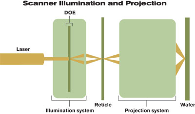
One of the main applications for DOEs is to enable resolution enhancement techniques (RETs) such as OAI in ArF (193 nm) and KrF (248 nm) scanners.Figure 4shows a schematic of the typical usage of DOEs in a scanner illumination system. OAI diverts light away from the axis of the scanner projection system, which increases the depth of focus to enable small feature sizes in manufacturing circuits. Before the use of DOEs, this was accomplished through the use of apertures that would be inserted to block the undesired portions of the beam. Since these apertures or "blades" are opaque in nature, they inherently cause a great deal of light loss, thus reducing throughput.
 |
|
4. In a typical scanner illumination and projection system, Tessera's Digital Optics is located within the illumination system to redirect the light striking the reticle into the desired locations. |
In addition, manufacturing constraints require support structures to be placed throughout the aperture to maintain its inner and outer structural integrity. As an example, for annular-type illumination, cross-hairs must be placed in the open annular region to support the central obscuration, resulting in further efficiency loss. Apertures are also limited in the complexity of the shape that can be machined. Small structures with irregular profiles can be difficult to create, so limitations are created on the size and shape of profiles that are feasible to manufacture.
The strength of the DOE as a resolution enhancement device is to redirect the light from undesired regions of the pupil into the useful target regions. This results in a much larger potential transmission efficiency, enabling higher throughputs.
The most critical difference between DOEs and apertures is the ability of DOEs to adjust the localized intensity of one region of the pupil, relative to another. Since apertures can only transmit or block light, they are limited to two intensity levels, unless half-tone techniques are used. As previously mentioned, the DOEs that Tessera manufactures have 255 discrete gray levels of intensity, which are defined by the target file and design process.
Other significant types of semiconductor manufacturing equipment that benefit from the use of DOEs include process control and wafer inspection equipment. These tools detect defects in unpatterned wafers, patterned wafers and reticles. DOEs are used to create very controlled, precisely shaped beam patterns, which enable these instruments to accurately and quickly detect nanometer-sized defects over a wide range of inspection points. Both brightfield and darkfield inspection systems use DOEs to provide the precise profile needed to enable high-resolution and efficient scanning.
The first use of DOEs in the beam path of brightfield or darkfield inspection equipment is to homogenize or smooth the input beam to provide uniform power distribution and aid in speckle reduction. The beam incident on the area of interest has to be very uniform to minimize false defect detection and maximize the inspection sensitivity.
Another application is to shape the beam in such a way that when it comes in contact with a defect, light scatters in the ideal profile to enhance the detection of defects. DOEs can also be used in inspection equipment to split the input beam into a specified pattern of multiple beams to enhance throughput and/or accuracy through redundancy. Multiple beams can also scan a single location in order to provide redundant feedback points to verify the defect.
The illumination path in mask inspection equipment is designed to emulate an actual optical scanner. The mask is illuminated by DOEs, as shown in the scanner inFigure 4. The mask image is then projected through a lens system and onto a test surface for evaluation.
The need to analyze the ever-decreasing size of defects will become more important as consumers demand smaller and more powerful electronic devices, which require freeform SMO to be adopted. The masks will become more pixilated with smaller and smaller assist features, making defect detection more difficult. The customized OAI that can be delivered by DOEs will be required to keep pace with this growing need. Historically, the use of OAI in inspection equipment lags behind cutting-edge scanner systems by at least one generation and is able to benefit from the developments established by scanner manufacturers.
Summary
The benefits that DOEs bring to the semiconductor industry have allowed them to gain widespread adoption. OAI enables the greater resolutions needed as feature sizes continue to follow the path of Moore's Law. With double patterning and SMO predicted to be the method of choice for the 32 nm and possibly 22 nm nodes, DOEs will play a critical role in providing the complex illumination sources that will be required.
In addition, the inspection and metrology equipment that is used to assist in the manufacture of next-generation designs will continue to employ DOEs as defectivity requirements continue to tighten. With reliable part-to-part repeatability and many more levels of complexity yet to be tapped, DOEs are well prepared to handle the requirements that will be placed upon them.
| References |
-
M. Himel et al., "Design and Fabrication of Customized Illumination Patterns for Low-k1 Lithography: A Diffractive Approach," Proc. SPIE, 4346, 1436 (2001).
-
J. Leonard et al., "An Improved Process for Manufacturing Diffractive Optical Elements for Off-Axis Illumination Systems," Proc. SPIE, Vol. 6924, 69242O (2008).
-
Y. Granik, F. Schellenberg, J. Carriere and M. Himel, "Manufacturable Source Mask Optimization," Microlithography World, Vol. 17, No. 4 (2008).
-
T. Coskun et al., "Enabling Process Window Improvement at 45nm and 32nm With Freeform DOE Illumination," Proc. SPIE, Vol. 7274, 72740B (2009). | |
|


