| About Us |
| News |
| Research |
| People |
| International Cooperation |
| Education & Training |
| Societies & Publications |
| Papers |
| Industrial System |
| Sitemap |
| Contact Us |
 |
 |
 |
 |
 |
 |
 |
 |
 |
 |
| Location: Home > News > Events |
| CMOS Transitions to 22 and 15 nm |
|
|
Scaling beyond the 22 nm node is likely to require fully depleted CMOS, either on SOI or bulk wafers. TSV 3-D interconnects and SiC stressors also appear likely to be implemented, while the jury is still out on when vertical finFETs and III-V devices will be widely implemented.
David Lammers, News Editor -- Semiconductor International, 1/1/2010 Technologists have long debated how far plain-vanilla planar CMOS transistors on bulk silicon wafers could be scaled. Now, the transition to new paradigms appears to be underway, with fully depleted CMOS almost definitely on the 15 nm roadmaps at IBM and Intel, with some form of vertical transistors being seriously considered as well. Mark Bohr, Intel's director of process architecture and integration, said he and his Intel colleagues are "pretty pessimistic that partially depleted (PD) CMOS will extend to the 15 nm node." A planar, fully depleted (FD) technology could only be constructed on a silicon-on-insulator (SOI) substrate, Bohr said, but a tri-gate or finFET device could be created on either bulk or SOI wafers. Gartner analyst Dean Freeman likens the current period to the early to mid-1980s, when first memory and then logic transitioned to CMOS. "The NPN transistor gave the CPU vendors a new lease on life. I think we are at a point like that again. But the question is out there: How do we keep innovating?"
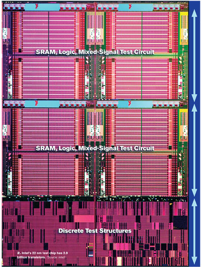
Strain also faces limits. More germanium can be added to the SiGe stressors — from the ~40% germanium level used at the 32 nm node — but there is less room for the material to create the strain. While IBM, Intel and others are thinning the gate dielectric with high-k materials, the gate dielectric "is not thinning as fast as we need it to in order to make an appreciable improvement in gate length scaling," said Bruce Doris, manager of advanced device integration at IBM's Albany, N.Y., R&D center. Other knobs are getting harder to turn as well. Operating voltages are leveling off, making it more difficult to reduce power consumption. Making the junctions shallower is causing the source/drain resistance to increase. What to do? At 22 nm, Intel will stay on a bulk technology, Bohr said. Intel is on track to introduce its 22 nm MPUs at the end of 2011. The Intel 22 nm test chip (Fig. 2) with SRAM arrays and logic peripheral circuits was introduced in September with a 364 Mb array size and 2.9 billion transistors. It includes a third-generation gate-last high-k/metal gate process that deposits both the dielectric and the metals at the end of the process.
Now working on pathfinding technologies for the 15 nm generation, Bohr said, "Fully depleted technologies have inherent low-power advantages." Intel is exploring a range of options, Bohr said, including tri-gate devices and fully depleted planar technologies. Intel has a decision to make in about six months, when it will lock in the process architecture for its 15 nm technology. (Scott Thompson, a former Intel technology manager who now teaches at the University of Florida at Gainesville, believes Intel will adopt a tri-gate structure at some point, while the rest of the industry will shy away from the manufacturing challenges of finFETs.) Historically, Intel has not been positive about SOI for partially depleted, planar CMOS devices. "We look for value," Bohr said. "Whether it is SOI or an extra metal layer, we do it if it gives us extra performance or lower power." John Pellerin, director of technology development for GobalFoundries, also said fully depleted CMOS is coming, though he said it is "difficult to draw discrete lines in the roadmap where such transitions occur." As a foundry that counts Advanced Micro Devices Inc. (AMD, Sunnyvale, Calif.) as its first customer, GlobalFoundries will support AMD and others with an SOI roadmap, while advancing bulk for other customers. Because so many companies are pooling R&D resources at the Fishkill Alliance, Pellerin said, "We do have the benefit of pursuing multiple architectures in parallel. Bulk is the incumbent for many applications, while for some high-performance sectors, PD-SOI is the incumbent. When those are dethroned is difficult to predict. What we do is look at novel architectures while at the same time raising the bar of the incumbents. That makes it more challenging for the newcomers." Partially depleted or conventional bulk transistors "become quite difficult" as scaling proceeds, Pellerin said. "In order to get the short channel characteristics required, certainly fully depleted device architectures — be they vertical devices like finFETs or planar SOI — allow you to take that challenge of channel control out of the equation. That's the enticement: not stuffing a lot of doping in the channel to control the short channel effect." The ability to get a consistent amount of doping in the channel is becoming difficult to manage. "That's where variation gets difficult," Pellerin said, "and where a fully depleted type of architecture starts to look very attractive." IBM, for its flagship MPU process technology, is considering making a move to fully depleted technologies as early as the 22 nm node, though it is more likely to come at 15 nm. Ghavam Shahidi, director of silicon technology at the T.J. Watson Research Center (Yorktown Heights, N.Y.), said IBM is developing fully depleted transistors, using planar structures on extremely thin SOI (ETSOI) wafers.2 ETSOI results in a thin silicon body, which reduces short channel effect (SCE) problems that stem from scaling the extensions to less than the depletion width. "Thin-body devices make the thinning of the extensions simpler, and they reduce the [gate-induced drain leakage] and Vt variations. The undoped body has much lower leakage and dopant variations," Shahidi said. PD-SOI involves learning to deal with the SOI history effect, which affects the Vt level and complicates design somewhat. With FD-SOI, there is no history effect, which makes FD-SOI design much simpler for smaller companies. The ETSOI technology incorporates several process innovations, including in situ doped epitaxial (implant-free) deposition of the source/drain and extension regions, and a faceted raised source/drain architecture, said Kangguo Cheng, lead engineer on the 22 nm device integration team at IBM's Albany R&D center.
ETSOI processing must be done carefully beacuse the thin silicon layer can recrystallize. "The silicon is so thin," Cheng said, "once you destroy the top silicon layer there is nothing left to recover." In situ doping, rather than implantation, is required, also to avoid material destruction.3 "We do in situ doping, which is non-destructive. We form the spacer, and need to leave the S/D epitaxial growth with the in situ dopants. After that, we heat up the wafer so dopants in the S/D can move toward the channel." A spike anneal does not destroy the silicon structure, he explained. While the ETSOI team is aiming for introduction at the 22 nm node ("All the ducks seem to be lining up," Doris said) the power of incumbency may keep IBM on partially depleted SOI until the 15 nm node. Pellerin, who manages the GlobalFoundries technology development team at Fishkill, said FD-SOI looks topographically similar to PD-SOI. "We are just dealing with a very thin body. It shares the processes we've grown accustomed to, and is good for channel characteristics." There is still the series resistance problem, and work is required to connect the source and drain to the channel. A raised S/D and other types of approaches have to be considered. "One challenge is: How do I reduce that parasitic resistance of that device?" Pellerin said. Gartner analyst Freeman said he believes that Intel and IBM will stick by their traditional guns, with Intel shying away from SOI substrates as long as possible and IBM pushing SOI as hard as it can. The Intel tri-gate structure, Freeman noted, "doesn't have to use SOI, because the area gets so small. There is still leakage at the substrate, but it is not a given that Intel has to go to SOI." Freeman's prediction is that "Intel will stretch bulk wafers as long as it can." IBM, on the other hand, will move as fast as is practical to fully depleted SOI. Both Soitec and Shin-Etsu Handotai (SEH, Tokyo) will be able to supply ETSOI wafers with the required specs, he said. FinFETs remain enticing FinFETs are another major path of investigation.3 Pellerin said ETSOI and finFETs also should be considered as a continuum, just as PD- and FD-SOI are. "I don't see one excluding the other. Both share some common advantages, and they also have their own unique set of integration challenges. To get to the transistor densities we will need, planar can only be shrunk so much. When we have to go to a finFET, it opens the door to an ability to achieve those transistor densities because we can pack vertical devices a lot closer together. FinFETs do have that additional knob of transistor density, to levels that planar would have difficulty in achieving."
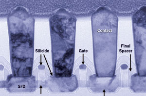
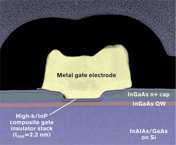
IBM doubled the number of R&D wafers on its finFET program in 2009 (Fig. 4), and the finFET effort is getting "really nice results," Doris said. "There are pros and cons of each one." A planar structure "is so comforting because it keeps the design style people are used to," he said. Although the width can be varied on planar transistors, with finFETs, "you have to add them up. There is no arbitrary width, so you quantize it and make more fins." Doris added, "I believe most people in the industry would agree that finFET processing is more difficult. Lithography is a huge challenge, though people can overcome that with sidewall image transfer." Etching the gate is another challenge. The gate wraps around the fin, making it difficult to characterize the profile of the gate. For there to be acceptable transistor characteristics, "the gate has to be as straight as possible," Doris said. In planar structures the gates lie in one plane, but "in finFETs, the gates are traversing the channel up and down all over your wafer. That poses some fundamental questions and approaches to how you integrate all the processes together to make that device," Doris said. When the gate wraps around the fin, it is difficult to optimize. "Much of the processing that the industry has used for the past 30 years can still be used on planar ETSOI," Doris said. "This industry tends to take very small steps. That's how we got to where we are. And that's why doing something fundamentally different like finFETs, at the same level of complexity, is hard to fathom in the near future." Pellerin said he has spoken to design customers about how prominent the design challenges to finFETs may be, in particular the "discretized device Ws." GlobalFoundries is targeting the 20 largest foundry customers, and they have not cited transistor width as a "showstopper or even a roadblock," Pellerin said. "We can offer multiple fins. Device designers don't use width as an analog kind of knob anyway. So while design with finFETs has been talked about, it is not panning out to be an issue at all." Freeman said although most companies are leery of finFETs because of the lithography and etching challenges of the vertical structures, "in one sense the epitaxial raised source/drain structures already are vertical in nature." SiC: yes or no? At 22 nm, it appears likely that one or more of the leaders will use the smaller-than-silicon carbon atoms to exert a tensile (pulling) stress on the silicon NMOS channel. The epitaxial structures on IBM's ETSOI process described at the recent International Electron Devices Meeting (IEDM), for example, use in situ doping to add SiC as a stressor on the NMOS devices. At the 2008 IEDM, and again at the 2009 Semicon West, the Fishkill Alliance partners, including Applied Materials, said they had demonstrated that SiC strain is workable. But has anyone committed to SiC? Pellerin said SiC is "an element we are looking at and considering for our 22 and below device architecture." Implanting the source/drain regions is becoming more complicated, and the SiC stressors are epitaxially grown, much like the SiGe strain regions on the pFETs. "Strain to the NMOS channel becomes another knob with which to improve performance," Pellerin said. Bohr has changed his tune somewhat on SiC stressors. In the past, he said Intel was leaning against SiC, but in an interview at the 2009 IEDM he said he didn't want to comment on the current status of SiC at Intel. Paul Packan, who presented Intel's 32 nm transistors at IEDM, also didn't reply to a question from the audience about SiC on the 32 nm NMOS devices. TSVs: Not only for memory Through-silicon vias (TSVs) and 3-D chip stacking are another technology that appears to be on the cusp of volume production. Already, IBM offers a fast SOI-based embedded DRAM capability, used on the Power 7 microprocessors and also offered to its foundry customers. TSV interconnected memory could be another weapon in IBM's unique technology arsenal of SOI, embedded SOI DRAM and, soon, TSV interconnects. Pellerin said TSVs will "definitely play a role" going forward, adding, "Embedded dense memory is an equally viable option and has a strong role to play. 3-D with TSVs is another approach to achieving that. And we shouldn't limit it to a logic chip mated to a memory. With TSVs, customers can really do heterogeneous types of integration that go beyond memory, enabling high-form-factor, high-function handheld devices. They can gain a lot of leverage in terms of what they can do in a small amount of space with heterogeneous die stacking using 3-D and TSVs." A role for heterogenous devices? By heterogeneous, Pellerin was referring to connecting logic with, say, optoelectronic or other devices that require a different material technology. Another meaning to the word heterogeneous is the use of a III-V transistor on the NMOS and a germanium transistor on the PMOS, for example. At the 2009 IEDM evening panel discussion, Krishna Saraswat, a professor at Stanford University, predicted that around the 10 nm channel length the industry will need to shift to new channel materials. Ideally, the industry will develop a decent III-V PMOS transistor to complement a III-V NMOS transistor, he said, a combination that would have "much lower power" consumption than silicon devices. "A III-V [NMOS] and germanium PMOS would be able to come in earlier that an all III-V solution, representing a good compromise," Saraswat said. Going forward, controlling power is the main challenge, said Raj Jammy, director of the front-end program at Sematech (Austin, Texas). "We need true high-performance devices with low power too. There is a blending or convergence going on," Jammy said, adding, "The beauty is that once we get to III-V devices, we can get to half of the operating voltages used today — to 0.5 V." Jammy led a Sematech workshop preceding IEDM on heterogeneous devices that combine a III-V (InGaAs is the most likely material set) device on the nFET, and perhaps a germanium channel on the pFET.4 The heterogeneous approach uses epitaxial techniques, depositing a III-V and germanium on a 300 mm wafer only in the critical circuits. For many university researchers, III-V-based devices are well-suited to the blending that may be needed. "III-Vs have made rapid progress in the last six months, more than many industry people realize," said T.P. Ma, a professor at Yale University. Some researchers, such as Akira Toriumi, now a University of Tokyo professor after a career at Toshiba Corp., argue that germanium channels can be used for both pFET and nFET devices.5 Jammy cautioned that "a germanium nFET is not easy, because of high contact resistance and high interface states."
Professor Dimitri Antoniadis, who heads up the Marco Center and device research at the Massachusetts Institute of Technology (MIT, Cambridge, Mass.), said III-V transistors "will help on the speed and power vectors; the density vector is tricky. They may not help on gate length scaling; there is a lot more work that needs to be done on scalability." Thomas Skotnicki, a research manager at STMicroelectronics (Geneva), raised doubts about whether III-V devices will ever be introduced into mainstream ICs. "Silicon gives us the speed we need. At best, III-Vs will be limited to high-speed paths. The high-mobility materials might be introduced locally to improve variability, which is a key problem." References |
