Speakers at the Nikon LithoVision event said EUV litho's slow development makes it unlikely that it will be in full, high-volume manufacturing use before 2019. Meanwhile, immersion lithography continues to be extended into increasingly smaller nodes, with Intel now expecting to complement 193i with either EUVL or E-beam maskless lithography.
Alexander E. Braun, Senior Editor -- Semiconductor International, 2/22/2010
Intel Corp. expects to complement 193 nm immersion lithography with either EUV or E-beam direct write lithography for the 11 nm generation, expected to arrive in 2015, said Yan Borodovsky, director of Intel's Advanced Lithography and Manufacturing Group.

Yan Borodovsky, Intel Corp.
Speaking at Nikon Corp.'s annual LithoVision event held the day before the beginning of the SPIE Advanced Lithography conference, Borodovsky said "complementing 193i with either EUVL or EBDW will allow 193i to be extended to 2015 and beyond, while keeping down process complexity and processing costs."
Complementing 193i with either EUVL or EBDW will allow the successful insertion of next-generation lithography (NGL). "With complementary patterning enabling the earliest use of EUVL in high volume manufacturing, the commercialization of maskless lithography for complementary use with 193i might be the next industry frontier," he said.
Borodovsky said 193 immersion lithography will be employed for both the 22 and 16 nm generations coming in 2011 and 2013.
Several other lithography experts at the Nikon event also looked into their crystal balls to see the shape of things to come for EUV lithography. Masato Hamatani, general manager of stepper design at Nikon, said EUV lithography, while full of promise, remains years away before it can be considered for high volume manufacturing. Nikon does not see EUVL coming into its own until well after the 16 nm node, possibly in 2019. While EUVL will be too late for the 22 nm half pitch, it should be available for some customer at 16 nm and beyond.
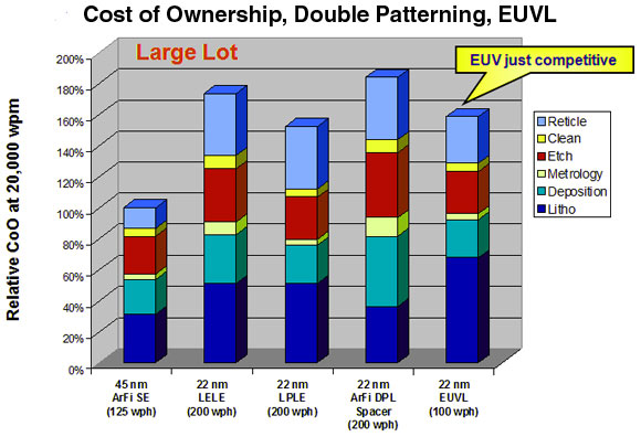
Double patterning and EUV lithography cost of ownership show that EUV is barely competitive compared to other technologies. Source: SPIE Litho Asia 2008.
"There are alternatives to EUV," Hamatani said. "There are ways to extend single patterning through source-mask optimization and custom illumination." Among the alternatives to enable the 32 nm half pitch and beyond are spacer double patterning, pitch-splitting double patterning such as LELE, LFLE, and line cutting lithography. Accurate and stable metrology is essential, including the use of encoder systems with interferometers to reduce errors. Double patterning is not nearly as expensive when compared to EUV," he said, concluding that "EUV still has many challenges."
Jeong-Ho Yeo, a principal engineer at Samsung Electronics Co. Ltd. (Seoul, South Korea), said he expects memory scaling to continue with double patterning and EUVL. However, Yeo said he does not view the multiple patterning option as an immediate solution because of its cost and complexity. "Low-cost double patterning is important for memory device cost reduction," he said. CD control is a challenge for double patterning, which may require a breakthrough technology. "Perhaps the necessary overlay can be achieved through platform performance or some kind of self-aligned concept."
Yeo said EUVL has proved capable of <20 nm resolution, as well as a 4X DRAM contact layer. Nevertheless, Yeo said he sees three top challenges for EUV: availability in the way of defect-free EUV masks; readiness in the resolution of a high power EUV source; and improvements in resist technology. "The blank defect level for high-volume manufacturing is <0.003/cm2 at 25 nm. There is still a large gap, with the current status at ~1/cm2 at 18 nm." In the resist area, the speaker pointed to crucial gaps for 22 nm half-pitch patterning, such as resist collapse, resolution, LWR, outgassing and sensitivity.
Takaharu Miura, a Nikon general manager, addressed EUV's lack of readiness for the next generation, indicating that for the moment it is possible to extend ArFi double patterning. "A high-volume manufacturing tool must be capable of providing multigenerational capabilities. An NA of >0.3 is required for the 22 and 16 nm half pitches, and >0.4 for 16 and 11 nm half pitch," he noted. Regarding the EUV source problem, Miura noted that system integrated performance with long-term operation is yet to be demonstrated. "In the mask sector, considerable improvement is needed," he said. "Actinic inspection and review tools are required."
Soichi Owa, a Nikon Fellow, said he expects to see immersion lithography extended down to 10 nm half-pitch SRAM patterns, through spacer quadrupling and line-cutting lithography. According to Owa, the challenges lie in negative tone resist, and reducing the mask costs for the multiple exposures that would be needed. Metrology is expected to play an important part in this process.
Kevin Lucas, a lithography manager at Synopsys Inc. (Mountain View, Calif.), said process and tool improvements have made pitch splitting double patterning a likely possibility for several logic and memory product nodes, focusing on contact and interconnect layers. However, for this to succeed, additional design and mask synthesis is needed. "Design rules are possible for memory and logic double patterning," he said. "While decomposition has improved to the point at which it can handle the complexity and scale needed for full chips." Lucas mentioned that tailored OPC and verification were increasingly important for double patterning to yield. "With appropriate design restrictions, more complete multiple patterning options can provide further shrinks."

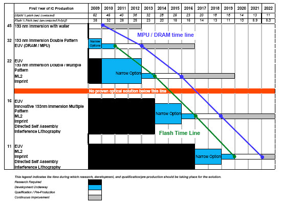
The 2009 ITRS edition forecasts several lithography tool solutions for different applications. (Source: ITRS)


