|
|
| TSMC Facing EUV, Wafer Cost Challenges |
 |
Text Size: A A A |
|
TSMC is ramping capacity for 40 nm production and preparing early production for 28 nm wafers, Shang-yi Chiang, senior vice president of R&D, said at a customer event in Japan. Expressing "shock" at the cost of EUV lithography, Chiang said TSMC is working to find "all the possible ways we can control costs for the tools, and to go to 450 mm wafers soon."
David Lammers, News Editor -- Semiconductor International, 3/1/2010
Taiwan Semiconductor Manufacturing Co. Ltd. (TSMC, Hsinchu, Taiwan) plans to double its 300 mm wafer capacity by the end of the year to meet 40 nm demand and is in preparation for volume production of 28 nm products, Shang-yi Chiang, senior vice president of R&D, said at a customer event in Japan.

Shang-yi Chiang, TSMC With a June target, TSMC is only four months away from early production of its 28 nm low-power devices based on an oxynitride gate stack. First introduction of the 28 nm high-performance (HP) process with a high-k/metal gate is scheduled for the end of September, followed by the high-performance low-power (HPL) process in December, also using a high-k/metal gate technology, Chiang said.
TSMC faced unexpectedly strong demand for 40 nm products in the early part of last year, and worked to resolve defects from the water-resist interaction in immersion lithography, as well as mechanical stability issues related to low-k dielectrics with a 2.5 k-value.
Chiang told the Japan-based customers that TSMC is building capacity very aggressively to fulfill the "very high demand from our customers" for 40 nm products, which accounted for 9% of TSMC's revenue in Q4 2009. The foundry expects that 40 nm revenues will more than double by the end of this year, accounting for almost 20% of sales. TSMC has worked with 60 customers thus far, with 61 products taped out and more than half of them in volume production now.

Revenues from 40 nm wafers will approach 20% by year-end.
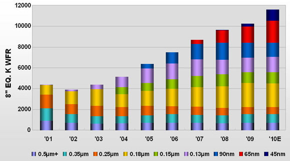
TSMC's Fab 12 in Hsinchu is readying additional 40 nm production now, raising total capacity to 80,000 300 mm wafers per quarter. Capacity will double by the end of this year, to 160,000 300 mm wafers per quarter, shared between Fab 12 and Fab 14 in Tainan, Taiwan.
Chiang said capacity additions are coming online much faster than a decade ago. When TSMC built the first phase of Fab 12, it took 16 months to finish the facility. "Now, for phase 4, we are able to do that in 12 months," he said. "After we build the shell and the facility is ready, we have to move in the equipment. For the tool readiness and tool delivery time and the tool installation time we are able to improve that by 33% in the last five years."

TSMC is doubling 300 mm wafer capacity this year. (Source: TSMC)
TSMC's 28 nm technology development team has achieved ~65% yields on 64 Mb SRAMs using the oxynitride-based LP process. For the high-k/metal-gate 28 nm HP process, Chiang said yields are ~26%, but said five months remain to improve the yields. For the 28 HPL process, 64 Mb SRAM yields are ~15% now, with early production beginning at the end of this year. "For the three 28 nm versions we are feeling quite comfortable, compared to our past experience at this stage of the development. We have high confidence that we are able to reach volume production yields smoothly."
Chiang said all five 28 nm shuttles are fully booked. "We are engaged with more than two dozen customers, and we expect the first 28 nm product tapeout in Q3 this year," he said. "Going forward to 28 nm, the biggest difficulty by far is the high-k/metal gate. It's really that way for everybody, with a lot of material issues."
At the customer event, Chiang said, "One challenge I'd like to share with you is the wafer cost. It's really steep." In previous technology transitions TSMC has been able to keep to a 15% increase in wafer processing costs. That will become extremely challenging from now on, he said, from both the device structure and lithography standpoints.
"If you buy one EUV tool with a matched track, it will cost about $80M for just one tool."
Because the EUV tools are relatively heavy, a special clamp is needed, attached to the fab ceiling to lift the EUV tool into place and for maintenance. "I was shocked to sign a purchase order a couple of weeks ago, a 1.9 million euros ($2.56M) purchase order for a clamp. This clamp is a custom-made clamp only for EUV. This tool is so heavy, no other tool can lift it up, and this custom-made clamp costs us 1.9 million euros, just to buy a clamp. It's really shocking."
If other costs increase like the lithography vector's, Chiang said, "Moore's Law will end very soon. Nobody will go to the new generation," he said. "It's not because of physics, it's because of cost. So TSMC will work very hard with our vendor partners, and we hope to find all the possible ways we can control costs for the tools and to go to 450 mm wafers soon. That will give us back more."
|
|


