| About Us |
| News |
| Research |
| People |
| International Cooperation |
| Education & Training |
| Societies & Publications |
| Papers |
| Industrial System |
| Sitemap |
| Contact Us |
 |
 |
 |
 |
 |
 |
 |
 |
 |
 |
| Location: Home > News > Events |
| Lotus Dreams: EUVL Continues to Approach Readiness |
|
|
As a follow-up to last week's SPIE Advanced Lithography conference in San Jose, Vivek Bakshi provides an update and his own perspective on the readiness of EUV lithography. He also offers insight into his confidence in ultimately winning a Lotus sports car from litho guru Chris Mack if EUV reaches high-volume production by 2014. Vivek Bakshi, President, EUV Litho Inc., Austin, Texas -- Semiconductor International, 3/2/2010
Attendance at this year's SPIE Advanced Lithography conference was up slightly from 2009, but the conference itself seemed a bit lighter. This year's EUV lithography papers were not part of an emerging lithography technologies subconference, but instead made up their own subconference to accommodate the increasing number of EUVL papers, which grew >50% over last year. On the Sunday before the conference, I taught a one day EUVL short course with my colleagues Patrick Naulleau and Jinho Ahn; our pre conference class not only was the best attended, we had to get extra chairs from next door to accommodate the overflow. Next month I will teach a two-day EUVL short course at ETH Zurich, with student attendance expected in double digits. So I look at all of these events as a sign of continued increasing interest in EUVL. EUVL is optical lithography Before reviewing the latest news from the conference, I want to clarify that EUVL is optical lithography. All principals of optical lithography clearly apply to EUVL, except that it is done in a vacuum environment with mirrors instead of lenses. During the EUVL short course, Patrick pointed out that reflection systems have a long track record in traditional optical lithography and that the multilayer mirrors used in EUVL are just quarter-wave stacks, which are widely used in lasers today. To that I would add that many semiconductor processing steps also use vacuum — film deposition, etch and ash, and implantation. So for fab engineers, vacuum-based processing is nothing new.
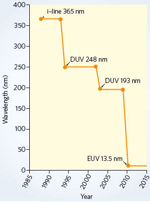
The software allows you to change the wavelength for printing a given feature, and see for yourself the simplicity of using 13.5 nm optical projection lithography to improve imaging quality, as contrasted with the increasingly elaborate techniques for 193 nm. Figure 1 shows how wavelength reduction for optical projection lithography has occurred frequently in the industry, with the switch to EUVL wavelength just a bigger change. Plenary talks Plenary talks for Advanced Lithography were given by Kazuo Ushida of Nikon, Sam Sivakumar of Intel, and Eric Chen of Silver Lake Partners. Chen finished his talk by redefining EUV as an acronym for "extremely undervalued." I cannot agree more, and see this as additional evidence of EUV acceptance.
Nikon believes that >0.35 NA optics is needed for a two-generation EUVL tool and sees EUVL being used at the 16 nm node. To extend 193 nm lithography, Ushida proposed a "line cutting" concept along with two sets of patterns on the same mask to make double patterning cost-effective. Intel's Sivakumar led us through an overview of the role of lithography in making chips, and pointed out the important part that next-generation lithography (NGL) will play in driving the interaction between process and design. Success also will depend on the choice of NGL and its cost-effectiveness. After the plenary talks, the conference was split into several subconferences. Although these meetings included a large number of sales pitches, there were some good technical talks to be found. In particular, I would like to commend Ahmed Hassanein and his group at Purdue for their fundamental study of tin plasmas for EUV sources, and Stan Stokowski of KLA for his talk on mask inspection technology. EUVL scanner makers Nikon is now in a comfortable second place and is focusing most of its efforts on designing an EUVL scanner for high-volume manufacturing (HVM), as it does not have a beta EUVL scanner ready for customers. Instead, Nikon plans to go straight to HVM based on learning from its alpha tool, EUV1 (a somewhat risky approach that may leave ASML with an even larger share of the market).
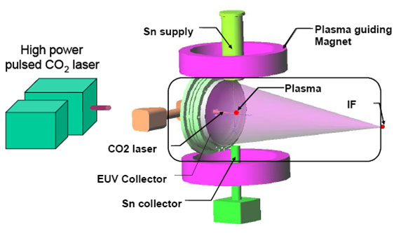
Nikon believes that its HVM EUVL tool will need 0.4 or higher NA. During Q&A, Nikon's Takaharu Miura pointed out the company is still working to achieve 0.4 NA with six-mirror designs in an effort to avoid an eight-mirror design, which would lose throughput because of additional reflective surfaces. ASML, the leading EUVL scanner supplier, continues to show good progress with plans to deliver its beta scanner, the NXE:3100, this year. I read a trade press headline saying, "EUV delayed again." I am not sure what this refers to, since ASML announced in 2009 that its NXE:3100 would be delivered in 2010, and appears to be sticking with that plan. In this year's presentation, ASML clarified EUV source power status, which I found to be very helpful. Traditionally, source power is reported at intermediate focus (IF) and many times it is an estimated power — which has occasionally raised questions about the readiness of source technology. ASML reported that NXE:3100 loses 20% of source power to dose control and will lose an additional 35% to the spectral purity filter (SPF) — thus reducing 200 W of "raw power" (i.e., measured power at IF and the current indicator of power specs for sources) to 104 W of "exposure power" (i.e., power available for printing). In other words, two new loss mechanisms were identified for source power, and it is "exposure power" that defines tool throughput. ASML is currently conducting acceptance testing at Cymer for a source that provides 20 W of exposure power, which corresponds to 15 wph throughput. ASML expects to get 40 W from Cymer's source this year to improve throughput to 25 wph, and the specs for the NXE:3100 are at 100 W for a 60 wph scanner. ASML showed data to prove that EUVL offers twice the depth of focus (DOF) and 30% feature size reduction over 193 nm lithography. Transmission of the NXE:3100 has been doubled since alpha demonstration, and an additional 50% increase (or 3× improvement) in throughput over ADT is planned for the HVM tool. ASML's HVM roadmap has 500 W of exposure power, and laser-produced plasma (LPP) EUV sources seem to be the only way to achieve that goal. ASML believes that EUVL is the only cost-effective technology for foundries, and noted that fab floor requirements for EUVL are 2× less than for double patterning. Silver lining in a tin cloud In my opinion, one of the most important papers of the conference was Cymer's clear status report on source performance. Cymer clarified that it shipped only two driver lasers for sources to ASML in 2009, and that its first source chamber will be shipped this quarter to ASML, after acceptance testing. The fact that Cymer's 20 W source will be available shortly made me a believer in the company's technology. Cymer has 40 and 100 W sources planned for 2010, with 1.5× improvement coming from laser power and 3× improvement deriving from conversion efficiency (CE) improvement. I believe there are good prospects that the 40 W source will be achieved this year, and that will be a significant achievement for Cymer and the EUVL community. This means that a beta EUVL scanner can be delivered in 2010, and a source upgrade in 2011 would have a good chance of bringing scanner performance toward 60 wph. This stepwise upgrade of light sources is nothing new — even for discharge-produced plasma (DPP) technology, sources were upgraded in phases to deliver full specified power of the alpha demo tool (ADT). During the conference, I discussed LPP issues with Hakaru Mizoguchi, CTO of Gigaphoton, the second largest supplier of EUV sources. I have always appreciated the lucid performance information from him and Gigaphoton. Figure 2 shows the schematics of Gigaphoton's LPP-based source design; the company currently has a 14 W prototype.
During our discussion, I became convinced that a combination of in situ cleaning and magnetic field-based control of plasma debris, combined with a gas curtain, has the potential to solve the tin debris problem in LPP-based EUV sources. In LPP, collector mirrors are directly exposed to a cloud of tin consisting of plasma, atomic and macro particle debris, making it difficult to integrate tin-based LPP sources into EUVL scanners. In DPP, a mesh "foil trap" helps protect the collection optics. The LPP collector design offers more light-collection ability due to a larger collection angle and better transmission because of the lack of a foil trap. However, foil trap designs have been proven for DPP and are currently in use; if necessary, they can provide the collector technology for LPP sources. So, based on this latest information and the likelihood of the Cymer source clearing its acceptance test this quarter, the tin LPP debris issue can be declared a difficult challenge and not a showstopper. And since tin debris was the main issue for LPP, high-power EUV sources also can be classed as a difficult challenge instead of a potential showstopper.
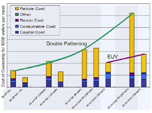
EUVL and chipmakers Samsung, Intel, GlobalFoundries, Hynix, Toshiba and TSMC are leading the development research for EUVL. Samsung wants EUVL ready by 2012, and TSMC announced during the conference that its has ordered an NXE:3100 tool from ASML. If this tool reaches its milestone of 60 wph as planned by 2011, I can see the next improved version being able to produce 100+ wph, which can get memory makers and foundries started with EUVL in the next few years to support printing of critical layers. In a keynote, Intel talked about extending immersion to the 22 nm node and about combining immersion with double patterning to support patterning at 11 nm. There was a strong correlation between Intel's presentation and the roadmap of Nikon, which has traditionally supplied Intel with scanners. However, Intel is also one of the leading chipmakers working on EUVL development, and has one of the most active EUVL research programs. Intel has invested more than any other chipmaker in EUVL early R&D over the past 10 years, and I think they will choose an NGL that is ready and cost-effective. So I see that the readiness of EUVL is driving the chipmaker's roadmap, and not other way around. EUVL and mask CoO In the conference news coverage, I read about complaints from some maskmakers that EUVL masks are expensive and leading adopters of technology have their own mask shops, so maskmakers will have to wait a long time to recover their investments. Masks offer a competitive advantage when everyone is buying the standard tool sets, and products and design are the main differentiators. With EUVL masks, cost is lowered if a single mask is heavily used. With time, I expect that a new business model will emerge to support the industry's needs in the area of EUVL masks, a familiar development for this business. Also, despite some press reports to the contrary, all the cost of ownership (CoO) analyses that I have seen show EUVL to be more cost-effective than double patterning, even with mask costs taken into account (Fig. 3).
Mask costs will differ between an in-house shop and an external supplier. In some recent analyses, the cost of double patterning is shown to be approaching that of EUVL, assuming a 200 wph throughput for a double patterning tool and only 100 wph for an EUVL tool.
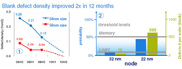
Actinic mask defect metrology Carl Zeiss showed its design for an AIMS tool for actinic inspection of EUVL mask defects, which the company expects to be ready in 2013. It is based on an EUV mirror optics design with a throughput of one mask per hour. It will need a 32 W/mm2 sr source, which Zeiss expects to be a DPP-based source. Zeiss is the supplier of EUV optics for ASML, and has good experience in designing and manufacturing EUVL optics systems. DPP source brightness is currently within a factor of 3×, so a target of 32 W/mm2 sr can be achieved (and maybe Zeiss can partner with ASML to speed up tool development). Energetiq is supplying a DPP source (with 10 W/mm2 sr brightness) to Mirai, which also showed the performance of its AIMS tool for actinic inspection. Lawrence Berkeley National Laboratory (LBNL) has a synchrotron-based tool that has supported actinic inspection research for many years, and researchers there proposed a bridge tool to continue helping the industry in the area of actinic inspection. Source brightness greater than what is currently available will be needed for actinic inspection of patterned masks, and I do not see any EUV source being ready in the near future to support these inspection requirements. HVM sources are not suitable for mask metrology tools because of their cost and size. KLA-Tencor, another company interested in providing an inspection tool, is also looking into actinic inspection and will probably try to further extend its 193 nm technology for EUVL mask inspection while actinic inspection tools are being developed. In other developments, Nano-UV, a DPP EUV source company, announced a joint venture with Lasertec for an actinic mask defect metrology tool, and newcomer Adlyte entered the EUVL market to provide LPP sources for actinic mask metrology. LPP sources are brighter than DPP sources, and I expect eventual sources for an HVM patterned mask inspection tool to be based on LPP or an alternative EUV source technology. I heard during the conference that actinic tools for patterned masks inspection are five or more years away. Even by then, I am not sure there will be sources with sufficient brightness to meet the currently specified requirements — so innovation has to come from new optics designs for metrology tools that relax source brightness specs. In any case, standalone AIMS tools are at least two to three years away, and until then mask defectivity inspection will be supported by the improvement of current capabilities of tools from Mirai, LBNL and KLA-Tencor, usage of send-ahead wafers, reduction of mask defectivity, and innovation. Yes, count on innovation — because that is what has kept this industry moving. It was pointed out in a Q&A session that plenty can still be done today to address mask defectivity — even without commercial actinic inspection tools — as there are copious detectable defects that need to be mitigated. After we see them clearly with actinic inspection, we will still need to mitigate them. Although 2× improvement in mask defectivity has been achieved (Fig. 4), much more must be done to reduce remaining defects. Ideally, most defects that require detection need to come from processing steps, and that is still not the case.
Resist progress Line edge roughness (LER) and resist collapse continue to challenge EUVL resists, as they will any technology used for 22 nm and beyond. ASML showed results for 24 nm L/S with 4.4 nm LER. For the 28 nm node, 81% of combined matrix of resist performance (M-factor) has been achieved. In any case, I was happy to see resist suppliers continuing to increase their engagement. Device results: You cannot get this with 193 nm
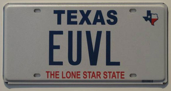
IMEC showed results of its success in modeling and correcting flare, and Toshiba revealed 1 nm variation in critical dimension (CD) over the entire wafer at 22 nm node patterning. The 2009 update of the International Technology Roadmap for Semiconductors (ITRS) indicates that there are no proven optical lithography solutions below the 22 nm node. I think that after seeing the 16 nm patterning results from this conference, the ITRS lithography working group will change its opinion. Dreaming of a Lotus Since my review of last spring's Advanced Lithography conference, much has been made of my bet with gentleman scientist and litho guru Chris Mack. (Chris is definitely a litho authority and I shamelessly recommend his book Field Guide to Optical Lithography every chance I get. Even if you are not a lithographer, this book is a very good investment.) The bet Chris made with me last year — that no abstracts on EUVL will be submitted for the 2011 SPIE Advanced Lithography meeting — was widely discussed at this year's conference, due in part to a presentation that showed a photo of a blue Lotus. I have to admit that it was an unfair bet; since then, many colleagues (some of them not even lithographers) have offered to submit EUVL papers in 2011 if I'll give them a ride in my anticipated new Lotus. However, we mustn't forget that although conference paper submissions do reflect industry interest in a given technology, even an increasing number of submissions does not guarantee success — the technology can still die a sudden death if it fails to deliver the goods. The semiconductor industry must find cost-effective solutions and will not hesitate to move on if an NGL technology does not perform per Moore's Law. EUVL must continue to show good progress, but in the wake of the Advanced Lithography conference, I am confident this will continue to be the case. There's another condition to the bet that says EUVL must be in high-volume manufacturing by 2014 for me to collect my prize. I think this will happen by then, and when the dust settles, history will judge EUVL to have been a common-sense extension of optical lithography. Chris will be recognized then as the leading enabler of lithography and its natural extension to EUVL because of his insightful books, Prolith work, years of educating lithographers, and contributions to effective control of LER. In the meantime, I have temporarily placed my "EUVL" custom license plates on my Suburban as I dream of tooling around Austin with those plates reassigned to my new Lotus.
|
