|
|
| Experts Detail 3-D IC Stress Management |
 |
Text Size: A A A |
|
Technology managers at a Sematech workshop discussed 3-D stress management issues. The creation of TSVs, die thinning, bonding and flip-chip packaging result in a 3-D chip stack with built-in stresses, which can lead to yield, electrical performance and reliability issues.Philip Garrou, Contributing Editor, Microelectronic Consultants of NC -- Semiconductor International, 4/6/2010
At a Sematech-organized workshop on stress management for 3-D ICs, technology managers addressed the need to simulate and measure the stresses being created by 3-D IC fabrication processes. The experts said there are reliability implications from stressors, and offered their suggestions how to minimize the impact of those stressors.

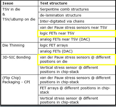
Test structures are needed to examine 3-D structures. (Source: IMEC) Defining the problem, Geert Van der Plas, principal scientist at IMEC (Leuven, Belgium) said, "TSVs, die thinning, bonding and flip-chip packaging result in a 3-D chip stack with built-in stress, which can potentially lead to yield, electrical performance and reliability issues." Van der Plas said insight into 3-D IC thermomechanical behavior requires analysis of test structures.
The stress on today's ICs is managed largely through design rules, and that approach must be extended to 3-D stacks, according to Riko Radojcic, principal engineer at Qualcomm Inc. (San Diego). He suggested that mechanical stress characteristics and consequences should be examined prior to, and during, the design cycle. Companies in the supply chain can provide layout rules, keep out zones (KOZ), die size, alignment, and PAD and CUP rules, he said.
The supply chain should standardize aspects of the design processes, including the process flow, handoffs and materials, and thermal budget and stress rules, Radojcic said. And vendors need to supply integration rules, qualification data, design kits, data on material properties and characteristics, and material constraints and thermal budgets.
The users, for their part, need to ensure compliance with rules, perform simulations to ensure compliance with target applications, and qualify the supply chain, Radojcic said. He proposed an EDA solution "that bridges package and silicon design and simulation environments without forcing re-tooling from the incumbent solution in either domain."
Xiaopeng Xu, a product manager at Synopsys Inc. (Mountain View, Calif.), detailed the use of his company's TCAD software to analyze 3-D structures. The different modules in TCAD can be used to extract 3-D parameters, as well as to predict interconnect stress distributions from multiple stress sources. The approach can detect stress hot spots that are susceptible to debonding, voiding and cracking, he said.
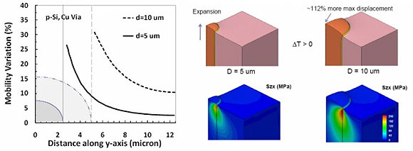
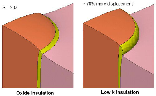
The presence of through-silicon vias (TSVs) appears to impact the mobility of p-doped silicon more than n-doped silicon, Xu said. Larger-diameter TSVs lead to larger mobility changes in silicon because of larger deformation and shear stress. The 3-D community also needs to pay significant attention to modeling, which reveals that low-k dielectrics with their inherent lower modulus result in less resistance to copper extrusion.

Larger-diameter TSVs lead to larger mobility changes in silicon because of larger deformation and shear stress. (Source: Synopsys)
Kamal Karimanal, technical account manager at Ansys Inc. (Canonsburg, Pa.), described how the Ansys Icepak computational fluid dynamics (CFD) software for electronics thermal management can be used to examine metal distribution and calculate temperature variations across a 3-D stack.

Low-k dielectrics are susceptible to temperature variations. (Source: Synopsys)
|
|


