|
|
| IITC Looks at Reliability, New Barriers |
 |
Text Size: A A A |
|
The 2010 International Interconnect Technology Conference (IITC) will focus on new barrier metal integration and reliability concerns. Planned for June 7-9 in Burlingame, Calif., IITC will look at the barrier metals that might succeed TaN and their impact on porous low-k dielectrics. Several research groups also looked at 3-D interconnects to see if the TSVs impacted transistor performance.
David Lammers, News Editor -- Semiconductor International, 4/5/2010
The 2010 International Interconnect Technology Conference (IITC) will take a broad look at reliability and process integration challenges presented by new barrier metals and 3-D interconnects. Planned for June 7-9 in Burlingame, Calif., the conference comes as many companies consider how to move past the combination of copper wires and tantalum-based barriers, insulated with ultralow-k dielectrics.
TaN barriers tend to oxidize from moisture from the ultra-low-k dielectrics. "Many people now believe that tantalum nitride could die at the next node, though companies of course will try to extend the incumbent," said Michael Armacost, an Applied Materials technology manager who serves as the publicity chairman for IITC.
Among these post-TaN papers is an IBM Research look at cobalt barriers with phosphorus caps, and a group from Taiwan Semiconductor Manufacturing Co. Ltd. (TSMC, Hsinchu, Taiwan) will examine the performance and reliability of a Cu-Mg combination at the 28 nm node.
The IBM and Lam Research team studied the reliability of a self-aligned cobalt tungsten phosphide (CoWP) cap that was deposited on top of a copper interconnect. The cap reduces electromigration, but can degrade the reliability of the porous ultralow-k dielectric. The team sought to determine whether this degradation can be prevented through various optimization techniques at the 32 nm generation.
Reliability is a thread running throughout all of the investigations of post-tantalum barriers, said John Iacoponi, a GlobalFoundries technologist and the North American program chair for the 2010 IITC. "Tantalum is not as plating-friendly as ruthenium, for example. But there are other challenges with these new metals," he said. "People are looking to make sure there are no voids, pinch points and other reliability issues. Definitely, at the 22-20 generation, there is more uncertainty facing the interconnect community."

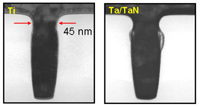
A slit void can be observed with the Ta/TaN barrier due to the stress associated with the shrinkage of the low-k film. A team of Panasonic and Renesas Technology researchers, for example, will describe the favorable interface properties of titanium, which shows good wettability for copper. The researchers investigated the interactions between titanium, TaN, low-k dielectrics and copper, and found that a thin Ti/TaN multilayer barrier could take advantage of the desirable properties of the materials.
This year, the program committee reviewed a fairly large number of high-quality papers on through-silicon vias (TSVs) and 3-D interconnects, Iacoponi said. An IMEC and KU Leuven team explored whether TSVs embedded in ultrathin substrates influence the operation and reliability of adjacent transistors. The researchers used a 130 nm CMOS process to fabricate copper TSVs with 5.2 µm diameters and 22 µm lengths. They placed the TSVs 1.1 µm away from the NMOS and PMOS transistors, in differing layouts.
The IMEC team, according to the paper's abstract, will report no performance degradation. Also, they saw negligible impact on carrier mobility from the stresses resulting from the thermal mismatch between the copper TSVs and the silicon substrates after extensive thermal cycling.

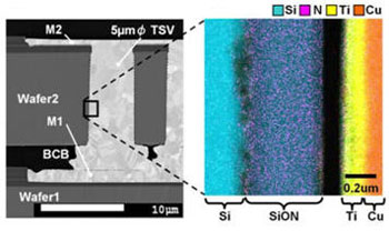
A cross-sectional TSV view (left) and a close-up of a sidewall. No copper atoms were observed in either the dielectric or in the silicon substrate. In another 3-D reliability investigation, Fujitsu researchers looked at bonded 3-D circuits and possible damage to the barriers used to protect vias from copper poisoning, a problem that can be worsened by the high processing temperatures needed to build TSV barrier layers. The Fujitsu team experimented with a relatively low-temperature plasma-enhanced chemical vapor deposition (PECVD) technique in a series of wafer-on-wafer experiments. The researchers built silicon-oxynitride (SiON) barrier films at various densities and thicknesses, at processing temperatures as low as 150°C. Their results showed no degradation in electrical characteristics or reliability for 45 nm generation transistors.
Sematech researchers looked at the wafer-on-wafer alignment accuracy, and will describe an alignment scheme aimed at submicron alignment accuracy for 300 mm wafers. The wafers were bonded face-to-face using thermo-compression bonding of the copper interconnects. The wafers were aligned using a newly developed aligning/bonding tool, which the Sematech researchers will describe at IITC. They also developed inspection techniques to verify the integrity of the bonds and to discover any voids. To better observe specific bonding structures, they developed a prototype integrated infrared high-speed focused ion beam (FIB) technique with CAD overlay capabilities.
Samsung researchers will describe an interlayer dielectric (ILD) technique they used with a 30 nm 1 Gb DRAM. First, they determined that the filling behavior of spin-on glass during spin coating is mainly dependent on the capillary effect. Then, they developed a wettable surface treatment to enhance filling, and optimized baking temperatures to minimize the viscosity of the glass. These techniques nearly eradicated the problem of contact bridges, they said, concluding that spin-on glass may be suitable for future memories.
The IITC kicks off with a keynote presentation by Intel Senior Fellow Mark Bohr, who will speak on "System Scaling: The Real Goal." Bohr will describe a recent shift in the goals for the semiconductor industry, from simply making ever-smaller transistors or chips with higher transistor counts, to integrating different systems into small packages for overall increased performance and power efficiency.
The 2009 IITC was held in Sapporo, Japan, part of an effort to draw more international attendees. Next year, the conference will be held in Dresden, Germany, May 9-13, in conjunction with the 2011 Materials for Advanced Metallization (MAM) conference. The committee plans to alternate between U.S. and non-U.S. locations.
|
|


