|
Embedded wafer-level ball grid array (eWLB) technology is evolving and can further optimize manufacturing costs beyond the current level through the adoption of larger panel sizes, according to Han Byung Joon, STATS ChipPAC's executive vice president and CTO.
Sally Cole Johnson, Contributing Editor -- Semiconductor International, 4/15/2010
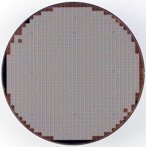
STATS ChipPAC (Singapore) has expanded embedded wafer-level ball grid array (eWLB) technology to reconstituted 300 mm wafers, and is the first to introduce 300 mm eWLB wafer manufacturing capabilities.

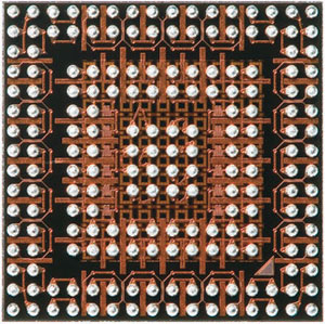
eWLB technology supports a thinner and smaller package. (Source: STATS ChipPAC) EWLB is a fan-out wafer-level packaging technology, introduced by Infineon (Neubiberg, Germany) in 2007, that uses a combination of traditional front-end and back-end manufacturing techniques. The approach involves processing all of the chips on the wafer in parallel, and provides a higher integration level, with a nearly infinite number of contact elements. When first developed, it also provided improved electrical and thermal performance, and a 30% reduction in dimensions compared with conventional lead-frame laminate packages.
In 2008, STATS ChipPAC, Infineon and STMicroelectronics (Geneva) formed an eWLB joint development partnership, with the goal of creating an industry-standard technology platform for cost-effective, highly integrated wafer-level packages.
Since then, STATS ChipPAC has invested >$100M in eWLB technology, and the company's current quarterly shipments are in excess of 30,000 reconstituted wafers, on target to achieve yields of 99% by the end of 2010.
Reconstituted wafers enable a fan-out WLP solution where the footprint is larger than the die size, while taking advantage of using an economically proven batch process, according to Han Byung Joon, STATS ChipPAC's CTO. The primary benefits of using eWLB are that it's a thinner and smaller package solution with superior board-level reliability that provides a high-performance solution for mobile phones and other handheld applications, Han said.

Embedded wafer-level technology enables all operations to be performed at the wafer level.
"EWLB technology is a robust package with copper and low-k compatibility and lead-free/halogen-free, green material sets. eWLB requires no substrate or bumping, which simplifies the logistics and supply chain — while lowering the manufacturing cost," he added. "Through our eWLB joint development partnership, we're working on a number of next-gen eWLB solutions, including those for 3-D applications."
The technology has already been proven and adopted by many mobile handset manufacturers to meet demands for increasingly complex, power-efficient semiconductor devices within an ever-shrinking package footprint. Han said that through its alliance with technology partners Infineon and STMicroelectronics, STATS ChipPAC jointly developed, and is now the first to manufacture, innovative eWLB technology such as side-by-side devices embedded in a package, ultrathin eWLB package and two-metal-layer distribution.
Roadmap for eWLB technology
The technology can further optimize manufacturing costs beyond the current level through the adoption of larger panel sizes, Han noted. "Technically, eWLB will evolve to integrate passives like inductors, resistors and capacitors into the various thin-film layers, active/passive devices into the mold compound and 3-D vertical interconnects, which opens up additional design possibilities for new system-in-package (SiP) and 3-D stacked packaging," he said. "3-D eWLB technology enables 3-D IC and 3-D SiP packaging with vertical interconnects, and can be implemented with TSV applications."
Han expects that a continued growth of capacity and transition to 300 mm wafer manufacturing will help position the company to deliver high-performance solutions at a lower cost in the future.
|


