|
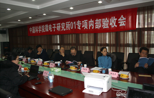
On January 13th, 2011, the evaluation show of Advanced EDA Platform Development project of “Key electronic devices—High performance IC design— Fundamental software development(KHF)” committed by EDA Center of Chinese Academy of Sciences (CAS) was successfully held at the Institute of Microelectronics, CAS. Experts from HHNES,Huada Empyrean software Co. , Fudan University, Tsinghua University, and Beijing Institute of Electronic Technology attended the conference.
At the beginning, Chen Lan—the director of this project—made a report about the technology and management of this project, and also showed the results and documents to the experts who were responsible for checking the achievements of this project before acceptance. These experts agreed that the main achievements of the project included the following four aspects:
1. Two sets of fully functional PDK under 130nm and 65nm technology node have been completed; also the methodology of PDK design and a design flow based on the homemade EDA tools have been established.
2. The research on DFM technology based on nanometer process has reached top level in domestic. Moreover two sets of DFM-friendly cellwise standard cell library based on the advanced process of 90nm and 65nm have been developed and also passed the DFM validation in Foundry.
3. Two chips are designed by homemade EDA tools, and the requirement, validation and improvement report of the EDA software has been proposed.
4. According to the SMIC 65nm process, a DFM application Flow has been established with the usage of the independently developed DFM software platform, lithography knowledge library and the third-party software.
The experts agreed that the project team had overfulfilled their target. They all agreed that the subject had passed the internal checking.
This is not only the first project that is accomplished and accepted since the specific projects of National Science & Technology were initiated, but also the first accepted project in CAS. This successful acceptance refines and sublimes the outcomes of research & development teams. Moreover, it is helpful for the final contract acceptance of the leading enterprises. The capability and experience of project management and project evaluation are significantly enhanced for EDA center and the institute of Microelectronics with the acceptance of this KHF project.
|


