|
Graphene is well acknowledged as potential material that promotes microelectronic technology in academia and industry, for its excellent physical characteristics and compatibility with silicon technology. Breakthrough progress has been made in the field of graphene-based electronic device by the graphene research group in the Microwave Devices and Integrated Circuits Department (Department 4th) of the Institute of Microelectronics of Chinese Academy of Sciences (IMECAS)in August 2011. Graphene-based electronic device with high performance was developed on a new type of graphene material grown separately by the methods of mechanical exfoliation for graphene-based device, epitaxial growth of SiC and chemical vapor deposition (CVD).
1. Mechanical Exfoliation Graphene-Based Device
(a) (b)
(c)
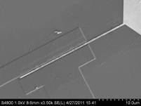
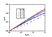
Fig.1. (a) Scanning Electron Microscope (SEM) Image of Graphene-Based Device; (b) Test Result of Graphene-Based Device; (c) Direct Current (DC) Characteristics of Graphene-Based Device. (Image by IMECAS)
Firstly, the research group got several hundred square microns of graphene material. Secondly, on this basis, they used compound gate dielectric structure in possession of intellectual property, developed thin-gate device technology, which solved the key technological problem in microelectronics devices. What’s more, they developed a complete process, which accomplished the preparation of graphene-based electronic device. As shown in figure 1, the performance tests show that the maximum cutoff frequency (ft) of this graphene-based electronic device is up to 18 GHz, which is the highest level in China.
2. Graphene-Based Electronic Device on the Epitaxial Growth of SiC
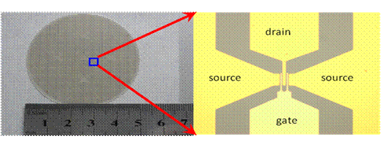
Fig.2. (a) Photo of Graphene-Based Electronic Device by the method of epitaxial growth of SiC (Image by IMECAS)

Fig.2. (b) Test Result of Graphene-Based Device (Image by IMECAS)
The research group developed a complete process for graphene dual-gate structure in possession of intellectual property, on 2- inches wafer graphene material grown by the method of epitaxial growth of SiC, which realized large-scale preparation of wafer level graphene-based device. As shown in figure 2, the performance tests show that the whole performance of this graphene-based electronic device is above GHz level, the maximum cutoff frequency (ft) is up to 4.6GHz, and the yield is above 90%. Furthermore, it is the first research group openly publicized by Chinese media which prepared graphene-based electronic device whose maximum cutoff frequency is above GHz level by the method of epitaxial growth of SiC.
3. CVD Graphene-Based Electronic Device

Fig.3. Photo and Test Result of CVD Graphene-Based Electronic Device (Image by IMECAS)
The research group realized large-scale preparation of wafer level graphene-based device on large area of graphene material grown by the method of chemical vapor deposition (CVD) on Copper foil. As shown in figure 3, the performance tests show that the whole performance of this graphene-based electronic device is above 500MHz, the maximum cutoff frequency (ft) is up to 1.1GHz, and the rate of finished products is above 80%. It is also the first research group openly publicized by Chinese media which prepared graphene-based electronic device whose maximum cutoff frequency is above GHz level by the method of chemical vapor deposition (CVD).
It is different from the original method of mechanical exfoliation for graphene-based single electronic device, to prepare electronic device on the wafer level graphene material, Its realization provides important basis for deep research into performance of devices with different feature sizes and graphene-based integrated circuits. It is also a prerequisite for large-scale preparation of wafer level graphene-based electronic device.
During the research of electronic device, much emphasis is put into the research and manufacturing of self-developed hi-tech products. The research group has granted for about 20 patents, published 1 paper in Applied Physics Letters (Volume 95/Issue 23/Nanoscale Science and Design : http://apl.aip.org/resource/1/applab/v95/i23/p233110_s1) and contributed several papers to international scientific magazines.
RESEARCHER CONTACT:
Researcher JIN Zhi
Institute of Microelectronics of Chinese Academy of Sciences
E-mail: jinzhi@ime.ac.cn
Website of Dept.:
http://english.ime.cas.cn/Research/ResearchDivisions/LAB4/
|


