Germanium has been considered as a promising channel material for high-speed, low power-consumption MOS devices because of its superior electron and hole mobility. For high-performance MOS devices, high-quality interface is essentially important to improve the mobility of MOS devices. Due to the poor stability of the high-k/Ge interface, there are large amount of scattering centers at the interface which are formed from the defects. These scattering centers become big obstacles to obtain high mobility, and thus strongly degrades the final device performance.
Aiming at this critical problem, the research group from Microwave Devices and IC department (Department NO.4) in the Institute of Microelectronics of Chinese Academy of Sciences (IMECAS), leaded by Prof. LIU Honggang, has realized high-quality interface with low defects density by employing chemical passivation on the Ge surface followed by Al2O3 deposition by means of atomic layer deposition in mid- September. On the basis of this method, they successfully fabricated Ge-pMOSFETs on Ge (100), Ge (110), and Ge(111) substrates, respectively. And the hole mobility has been considerably enhanced (Fig. 1). Especially on Ge(111) substrate, the peak mobility up to 660 cm2V-1s-1 has been achieved through HCl-chemical passivation, which is 3.5 times higher than the bulk silicon and come up to advanced world standards. Moreover, under the collaboration with Prof. Toriumi's Group from The University of Tokyo, Prof. LIU's group has systemically investigated the reaction mechanisms at the high-k/Ge interface by using XPS characterization. For the first time, the kinetic model of the GeO disproportionation (2GeO→Ge+GeO2) and the redox reaction at the GeO2/Ge interface has been elucidated (Fig. 3).
The results had been published in Applied Physics Letters, Chinese Physics Letters and Solid State Devices and Materials:
1. S. K. Wang, H. -G. Liu, and A. Toriumi, Kinetic Study of GeO Disproportionation into GeO2/Ge System using X-ray Photoelectron Spectroscopy, Appl. Phys. Lett. 101, 061907 (2012)
2. B. Q. Xue, H. D. Chang, B. Sun, S. K. Wang and H. -G. Liu, The impact of HCl precleaning and Sulfur passivation on the Al2O3/Ge Interface in Ge Metal-Oxide-Semiconductor Capacitors, Chin. Phys. Lett. 29, 046801(2012)
3. S. K. Wang, B. Q. Xue, H. L. Liang, Z. X. Mei, Y. Li, W. Zhao, B. Sun, X. L. Du, and H. -G. Liu, Growth of Epitaxial Beryllium Oxide on Ge (111) by Molecular Beam Epitaxy. Accepted by Ext. Abst. Int. Conf. On Solid State Devices and Materials (SSDM 2012), (Sep 2012, Tokyo)

Fig. 1 The Relationship between Effective Hole Mobility of Chemical-Passivated Ge-pMOSFETs and Substrate Effective Carrier Density with the Substrate Orientation of Ge(100), Ge (110) and Ge(111).(Image by IMECAS)
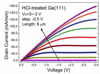
Fig. 2 I-V Characteristic of Chemical-Treated Ge-MOSFET with Ge (111) Substrate.(Image by IMECAS)
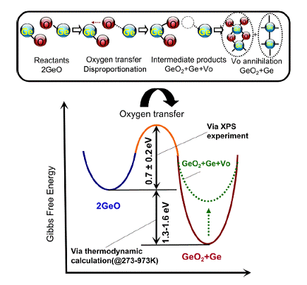
Fig. 3 Kinetic Model of GeO Disproportation and the Redox Reaction at the GeO2/Ge Interface.(Image by IMECAS)
RESEARCHER CONTACT:
Researcher LIU Hougang
Institute of Microelectronics of Chinese Academy of Sciences
E-mail: liuhonggang@ime.ac.cn
Website of Dept.:
http://english.ime.cas.cn/Research/ResearchDivisions/LAB4


