Nowadays, the shortage of traditional energy source and the pollution to the environment are getting worse. Therefore, new energy industries have drawn a lot of attention for the advantages of energy-saving and environment protection. Among the new industries, battery packs of high power are facing large and increasing demands. To meet the high power demand, tens and even hundreds of cells are usually connected in series in a pack. During the charging and discharging processes, because of the diversities of the cells, the difference in behaviors of the cells can be enlarged. Consequently, the available charge in the whole battery pack decreases and the life of the battery pack is shortened. Based on the above analysis, battery management system (BMS) is often equipped to monitor the parameters and states of the battery pack. The battery stack monitor chip, as the core part, determines the performance of BMS.
With the support of National Science and Technology Major Project and also Major Support Projects for the national strategic new industry of the Chinese Academy of Sciences, the ASIC & SYSTEM Department of Institute of Microelectronics of Chinese Academy of Sciences (IMECAS) conducted some research on key technologies of the battery monitor chip. The chip BM303 was finally developed. The chip was designed with functions of high accuracy data acquisition, high reliability, stacked and level-shift communication, real-time monitoring, controlling of cell equalization. One single chip can monitor 8 cells in series. for tens or even hundreds of cells, a group of chips can be stacked and communicate with each other through high voltage communication interface. There are high precision analog circuits such as a delta sigma converter with built-in noise filter, and large scale digital logic control circuits integrated into the chip.
The packaged chip is shown in Fig.1. Fig.2 shows the die photograph of the unpackaged chip.
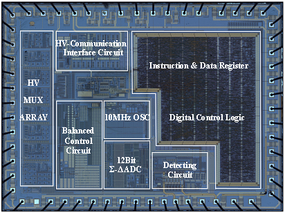
Fig.1 Chip with LQFP44 Package (Image by IMECAS)
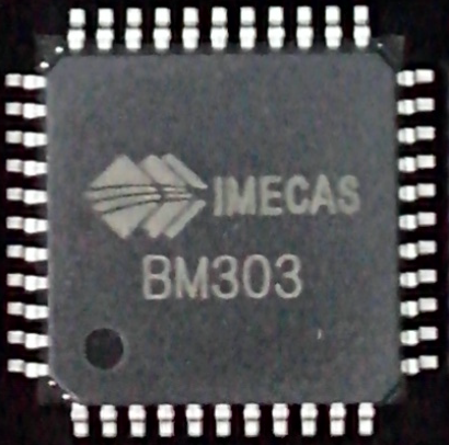
Fig.2 Photograph of Bare Chip(die) (Image by IMECAS)
The research team dealt with a series of difficulties, including data acquisition under high common mode voltage, communication and cooperation mechanism, special ESD design, high precision voltage reference, high precision ADC converter, equalization control and digital logic control, and finally a manufactured chip was achieved. The test showed that the maximum total measurement error is 2.1‰.The cells can be equalized either with the switch buried inside the chip, or by the discrete components outside driven by the chip. For the application that demands more than one chip, the chips can be stacked and communicate with each other in a shift-level way. Besides the data acquisition function, the chip can offer the fault detection for cells, making it possible to monitor and manage the battery pack intelligently. In the reliability test, the designed chip passed a series of ESD tests, including the voltage of 2000V(Class 2) test in HBM, 1000V(Class 4) test in CDM and 200V(Class 2) test in MM.
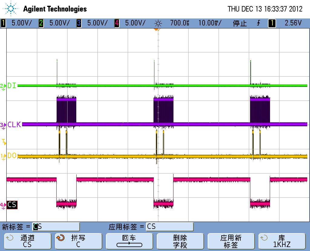
Fig.3 Communication Wave of Uploaded Cell Data (Image by IMECAS)
Fig. 3 shows the cell data information read from the monitor chip, which is uploaded to the MCU through SPI interface so that the voltage can be calculated.
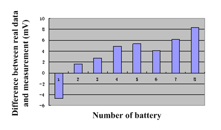
Fig.4 Voltage Measurement Error(Image by IMECAS)
Fig.4 shows the voltage measurement error of 8 cells (Maximum 0.21%, minimum 0.04%). An error of 2mV in voltage measurement means 1% error for the estimation of SoC(system on chip), so the results indicate that, in the worst situation, a 4% error of SoC estimation can be achieved, this is much less than the 10% demanded in real application. The chip and the system developed from it can be applied to the electric vehicles and tools, battery energy storage system.
It is proved that the performances of the chip have reached the leading domestic level, and samples can be offered for engineering application, with specifications and user manuals available. At present, the chip and its system are in promotion for product level application. Based on the new break for a series of key technologies in battery monitor chip mentioned above, the research team will further research on the analog-digital mixed chip for battery packs, aims to make some breakthrough in core technologies of battery pack’s intelligent management and to lay a foundation for localization and industrialization.
CONTACT:
Researcher HEI Yong
E-mail: heiyong@ime.ac.cn
Website of Dept.:
http://english.ime.cas.cn/Research/ResearchDivisions/LAB2/


