Recently, researchers at Integrated Circuits Advanced Center (ICAC), Institute of Microelectronics, Chinese Academy of Sciences (IMECAS) achieved a significant breakthrough in novel gate-all-around silicon nanowire (GAA SiNW) MOSFET’s structure and manufacture technology for core devices in sub-5nm node integration circuits (IC) developments.
The FinFETs applying in current mainstream IC manufacture are to meet lots of challenges while IC scaling into 5nm node and beyond. New device structures such as GAA NW or stacked NW transistors with excellent channel electrostatic integrity, leakage control abilities and one-dimensional ballistic transport specialty have attracted increasing interest and been considered to be the most promising core device candidates beyond traditional FinFET, In recent years, the research and development on next generation GAA NW transistor by implementing ideal GAA NW structure into the mainstream FinFET manufacture process is becoming one of the top tasks undergoing by various international IC R&D institutes. As shown in Figure 1, two different main technologies, named in stacked NW (IMEC, 2016 VLSI) and stacked nanosheet (IBM, 2017 VLSI), are reported and both devices are fully compatible with conventional HKMG FinFET flow. These technologies have similar integration scheme by epitaxy growing multi-layer Si/SiGe stack layers and releasing NW channels in RMG process with selective etch to SiGe or Si films. As a result, the real stacked NW transistor is with the GAA NWs distributed only in the channel and the fin shape remaining in SD regions. However, these approaches are facing some important technology challenges for large scale IC applications, e.g. requiring extremely sophisticated multi-layer Si/SiGe epitaxy process with nearly defect-free film quality; low process thermal budget (~700 oC) and possible contamination issues of Ge-atom out-diffusions in later integration steps.
In order to overcome these issues mentioned above, a new device and manufacture approach, named in totally isolated GAA NW MOSFET are firstly proposed and finished by the research team of Professor Huaxiang Yin from ICAC of IMECAS. The novel device is also fully compatible with conventional HKMG FinFET process. On bulk-Si, the polygonal fins isolated to the substrate were formed with advanced etch technology and linear oxidation process. After NW release with wet-etching of SiO2 in the RMG process and then the fins were transformed into the circular and inverted droplet NWs by using H2 baking and oxidation processes, respectively. The NW channel has the perfect Si crystal quality and few defects due to the formation by the bulk Si substrate. The optimized NW devices with Lg = 16 nm demonstrate superb SCE immunity characteristics, with SS = 61.86 mV/dec and DIBL = 6.5 mV/V for the inverted droplet NW device. These results are very close to the ideal limits of MOSFETs and are the best reports for similar devices in recent reports. They are also far better than those of FinFETs with similar fabrication process. Moreover, the new approach is capable of making a novel stacked NW device and the research is undergoing now. The relevant patents of the novel device structure and fabrication technologies have been authorized both in China and America, and the intellectual property rights will be protected by law in future. As a result, the new approach supply one different choice for sub-5nm IC developing in China with self-developing core-device architecture and manufacture technology.
This work entitled《Novel GAA Si Nanowire p-MOSFETs with Excellent Short Channel Effect Immunity via an Advanced Forming Process》is published in IEEE Electron Device Letters (doi: 10.1109/LED.2018.2807389), the most famous international academic journal in the microelectronic device field.
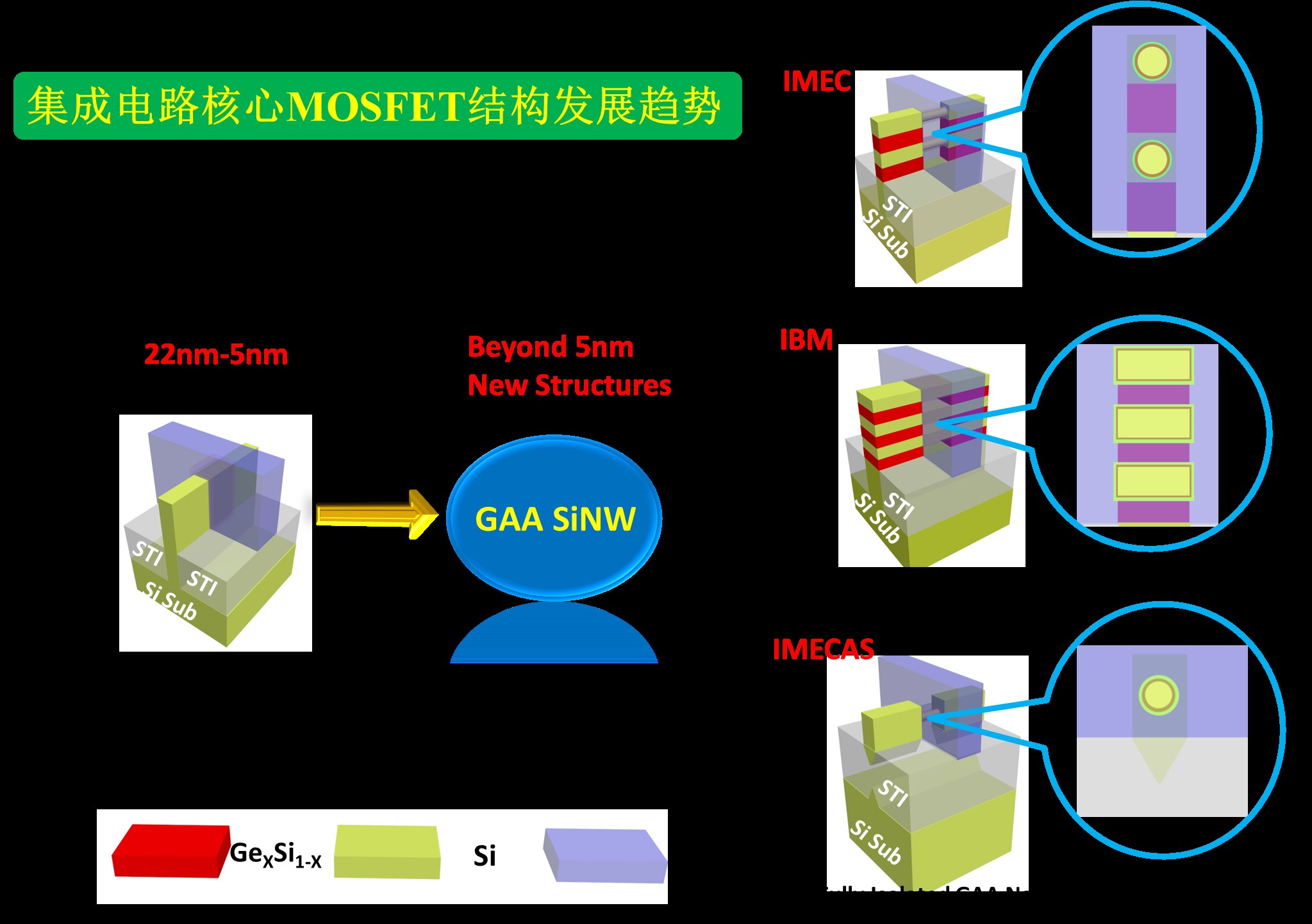
Fig. 1. The development trend of core MOS device structure in IC
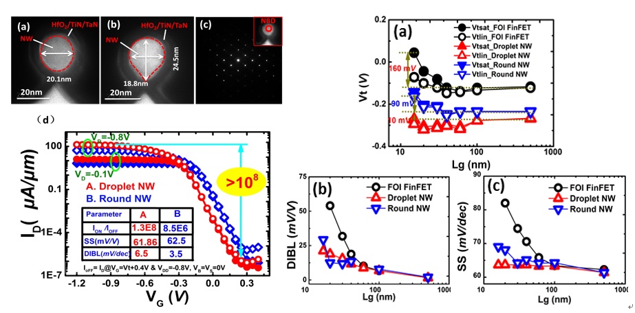
Fig. 2. The device structures and electrical properties of the fabricated fully isolated GAA Si NW p-MOSFETs


