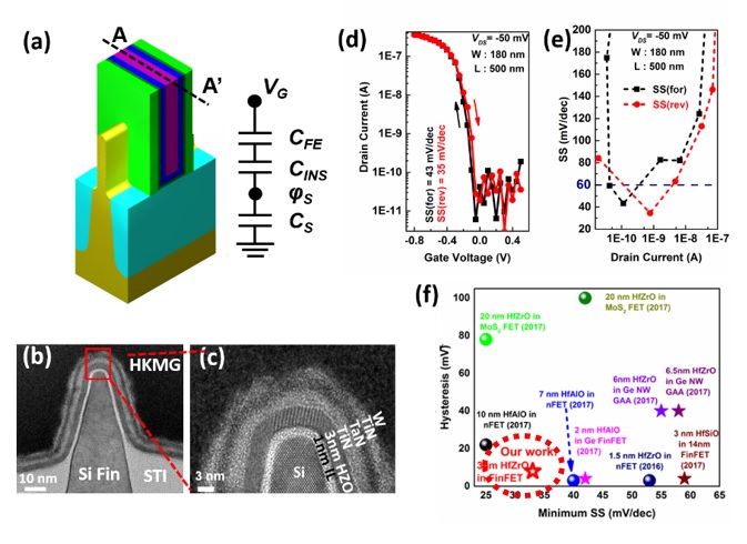
A physical limit of Boltzmann tyranny renders the subthreshold swing (SS) of a Si-based transistor no less than 60 mV/dec at room temperature, which leads to the reluctant reduction of power consumption, especially when Complementary Metal-Oxide-Semiconductor (CMOS) technology into sub-5 nm nodes.
By integrating ferroelectric materials in the HKMG process, differential negative capacitances (NC) can be realized to break through the traditional Boltzmann tyranny and obtaining a steeper SS. Consequently, a smaller supply voltage and power consumption can be employed for the operation of IC.
Even some progress has been made in recent years, the exploration of novel ferroelectric materials in mainstream FinFETs is, however, still in the inception phase.
Researchers from Integrated Circuit Advanced Process Center (ICAC) of Institute of Microelectronics, Chinese Academy of Sciences (IMECAS) have developed new processes for the growth of Hafnium Zirconium Oxide (HZO) and integration in FinFETs etc. High performance NC p-FinFETs of different gate lengths featuring with an ultra-thin 3-nm-thick ferroelectric HZO are demonstrated.
In detail, both the atomic-layer deposition (ALD) process and post-annealing process have been carefully modulated during the growth of ultra-thin HZO. Thanks to the low interface defect density and appropriate engineering of capacitance matching, as-fabricated FinFETs show greatly improved SS values i.e. 34.5 mV/dec with 500 nm gate length (LG) and 53 mV/dec with 20 nm LG, and small hysteresis voltages i.e. ~9 mV with 500 nm LG and ~40 mV with 20 nm LG. The SS is much smaller than Boltzmann tyranny of 60 mV/dec and the hysteresis voltage is well controlled to an acceptable level. The ratio between Ion and Ioff is as high as 1.23×10⁶.
NC FinFETs in this work pave a way for developing core transistors with almost identical performance while remarkably lowered power consumption in the future.The latest results have been entitled“FinFET With Improved Subthreshold Swing and Drain Current Using 3-nm Ferroelectric Hf0.5Zr0.5O2 ” in a prestigious journal “IEEE Electron Device Letters” .
This work was financially supported by the National Science and Technology Major Project 02 and the National Key Research and Development Program.

Fig. 1 (a) 3D schematic of NC FinFETs; (b-c) TEM images of NC p-FinFETs across AA’ directions; (d) Measured IDS-VGS curves of NC p-FinFET, where steep average SSfor and SSrev of 43.2 and 34.5 mV/decade are achieved, (e) extracted SS as a function of the IDS of the device in (d); (f) comparison between our work and reported NC FETs from other groups. (Image by Prof. YIN’s group)
Contact:
Prof. YIN Huaxiang,Ph.D Professor
INSTITUTE OF MICROELECTRONICS OF CHINESE ACADEMY OF SCIENCES
E-mail:yinhuaxiang@ime.ac.cn


