Recently, the 2020 IEEE International Electron Devices Meeting (IEDM) was held in a fully virtual format. At the meeting, the research team of Liu Ming from Institute of IMECSA presented the latest research results in the field of resistive memory chip integration.
Resistive random access memory (RRAM) is considered as a strong candidate to replace e-Flash in advanced process nodes due to its advantages of good compatibility, excellent scalability and high reliability. However, whether it can be integrated into the 10 nm logic process platform is a key factor affecting the future market of RRAM.
The scientific research team led by Academician Liu Ming demonstrated the RRAM integration on the 14 nm FinFET logic process platform for the first time, and realized the embedded RRAM memory chip of 1Mbit. The 1T1R cell area is 0.022um2, and the memory density of the chip is 13.4 MB /mm2. In view of the voltage mismatch between RRAM devices and logic units, the team proposed a programming scheme of negative voltage bias. By introducing a deep N-well, the negative voltage could be applied at the memory array without forward bias of PN junction. This programming scheme could reduce the absolute value of applied voltage reduce along the transmission path and thus reduce the risk of high voltage risk.
Furthermore, the team ultilized an optimized array architecture to reduce the risk of transistor breakdown. The operating voltage, programming current, and RC in BEOL were important factors affecting the scalability of the RRAM technology. The team proposed a possible design rule for RRAM integration at sub-10 nm process node. To improve the storage density, an array architecture of 1T2R could be adopted judiciously. This work has a certain guiding significance for improving the embedded application of RRAM in advanced process nodes.
The paper "First Demonstration of OXRRAM Integration on 14nm FinFET Platform and Scaling Potential Analysis towards sub-10nm Node" based on the above research results was selected into 2020 IEDM. Xu Xiaoxin, associate professor of the Institute of Microelectronics, is the first author of the paper.

Fig. 1 (a) Schematic of the RRAM structure integrated on the 14nm FinFET platform. (b) TEM cross-sectional image of RRAM unit. (c) the logic devices with the 2 Finger structure. (d) The stacked structure of RRAM.(
(Image by XU’s group)
)
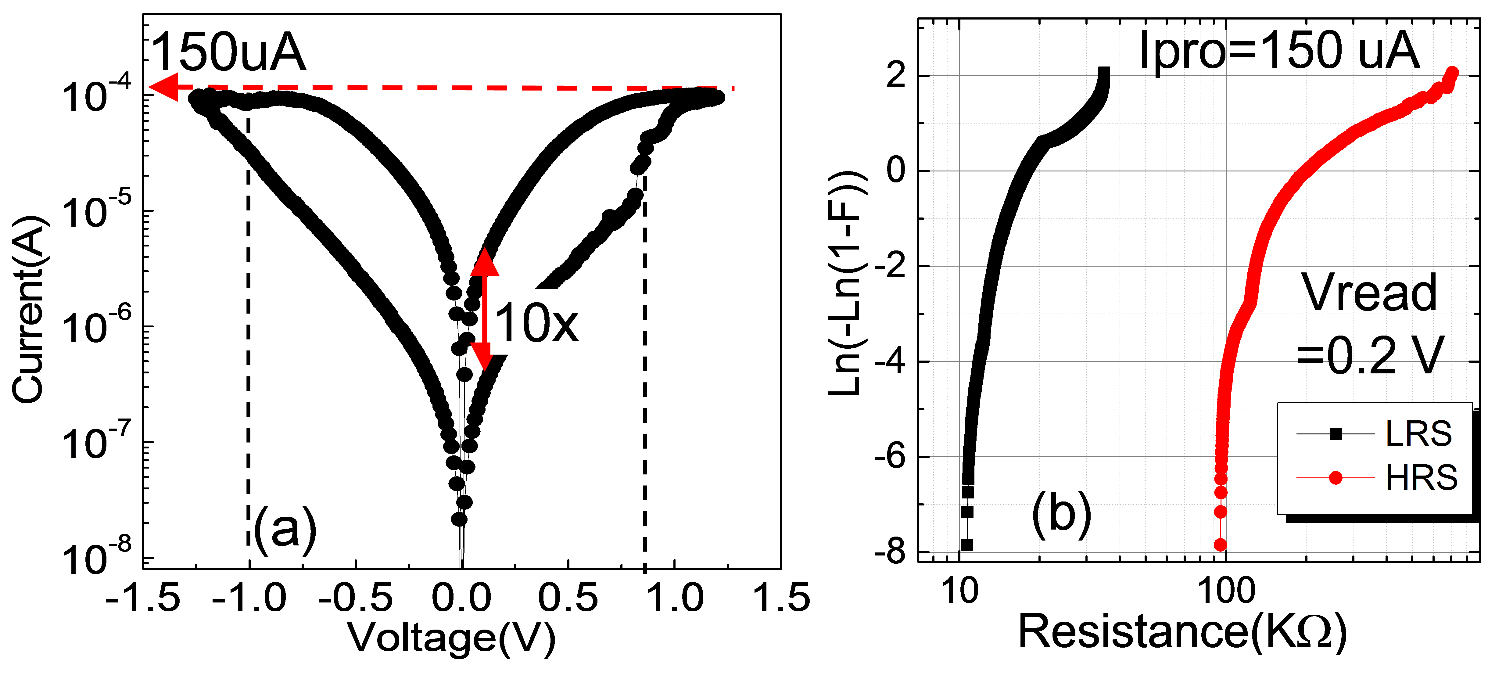
Fig. 2. The basic characteristics of the RRAM. (a) IV curves. (b) Distribution of the RLRS and RHRS adopted from 4Kb array.(Image by XU’s group)
Contact:
Associate Researcher XU Xiaoxin
Key Laboratory of Microelectronic Devices Integrated Technology, CAS
E-mail:xuxiaoxin@ime.ac.cn


